Electronics are only as valuable as their uptime, as scheduled or (especially) unscheduled maintenance can significantly hamper business operations or end-user satisfaction. However, the nature of electronic systems means continued usage or high-stress applications can quickly degrade performance and service life. One of the best ways to combat reliability issues is to employ a full slate of inspection criteria and tests along with a robust set of design for manufacturing (DFM) standards that ensures electronics are capable of meeting their expected level of rigor. PCBA reliability testing aims to limit defects with pass/fail inspection criteria and stress test results. VSE’s commitment to quality control (QC) aids designers with long-lasting service lives for demanding conditions.
PCBA Reliability Testing by Type
| Tests | Test to Failure? | Service life affected? | |
| Fabrication |
|
No | No |
| Assembly |
|
No | No |
| Stress test |
|
|
|
| Functional Testing |
|
|
|
PCBA Reliability Testing Overview
Fabrication Testing
Because electronics manufacturing is a complex multi-step process, inspection and testing must be ongoing throughout the different sub-stages of production. Starting with fabrication, the board undergoes several checklists that ensure basic resilience:
- Visual inspection – Inspecting the board post-fabrication or post-assembly allows technicians to confirm the presence of common defects by checking for typical visual irregularities. X-ray inspection can peer underneath dense pinout packages like BGAs or between board layers for greater clarity.
- Automated optical inspection (AOI) – Similar to visual inspection, it uses cameras and known-good comparisons to inspect at higher volumes. Compatible with deep learning models.
- Peel test/delamination – Checks for the presence of delamination (separation of board layers) at the edge of the board or bubbles within the board area. Different board materials will have different peel strengths and standard laminates may not be suitable for stressful environments.
- Continuity test – The test checks for opens (infinite resistance) and shorts (zero resistance) across the board according to the netlist generated from the schematic.
- High-potential (Hi-Pot) test – Given a high enough voltage, the dielectric between conductors can break down, producing an electrical arc that can damage components or the board. High-voltage PCBs or boards with thin dielectric layers should use this test to confirm the validity of the layout and stackup, respectively.
Assembly Testing
Assuming the board is mechanically sound, the board moves to assembly. Assembly joins the various components of the BOM to the board with a well-formed solder joint that is mechanically rigid and electrically contiguous. Depending on the package type – surface mount device (SMD) or through-hole (TH) – designers can use solder reflow ovens or wave soldering to rapidly and efficiently bond the components to the board. Larger or irregularly shaped components may require manual hand soldering by a trained technician. Once assembled, the board requires a new round of testing to validate build quality:
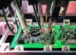
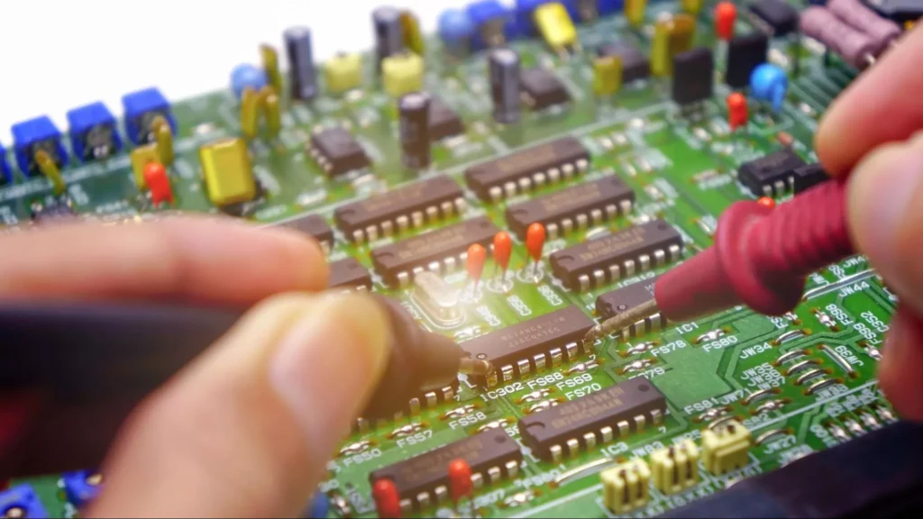
- In-circuit testing – ICT measures the voltage/current throughout the circuit after installation using test points placed by the designer; the test methodology can either use a programmable flying probe configuration or a customized test fixture (AKA bed of nails). ICT can also detect component failure by simulating voltage/current inputs and comparing outputs to the expected logic.
- Time-domain reflectometry (TDR) – One method of measuring impedance values of traces uses a signal’s reflections as it encounters the various discontinuities along its path. Depending on the shape of the reflected waveform, designers can adjust the trace to account for parasitics that can affect timing in single-ended lines or differential pairs.
Stress Testing
The last class of reliability testing focuses on methods that simulate extreme operating conditions and extended service life operations to weed out early failure. Like most manufactured devices, PCBs follow a “bathtub” curve: a higher failure rate earlier and later in the service life, separated by a stable “mid-life” period. Therefore, stress testing boards can remove early failures, improving end-user satisfaction:
- Thermal shock testing – Exposes the board to temperature extremes, typically for a short period. These extremes can mirror outdoor environments or high current draw leading to excess thermal dissipation.
- Highly accelerated life testing (HALT) – HALT evaluates use conditions and device longevity. Although the test proceeds to failure, it does not aim for failure conditions; instead, it provides data to estimate the failure points.
- Burn-in testing – Burn-in is the “warmup” period for the assembled circuit, ensuring all components operate correctly when powered up to avoid device infant mortality. While burn-in testing is necessary, it reduces a device’s service life in all cases. Therefore, minimal burn-in time is key to optimizing QC and service life.
- Environmental testing – Heat is the enemy of electronics, but other environmental factors can also reduce a board’s service life. Moisture or particle ingress and vibration can lead to shorts, opens, and mechanical damage to the board.
Functional Testing
- Manual functional testing – Testing with basic instruments like multimeters and oscilloscopes to verify basic functionality.
- Fault simulation – Use of software to model PCB behavior when certain faults are introduced, helping to identify potential issues before physical testing.
- Adapted cable testing – Use of specialized adapters or fixtures to connect a cable assembly to a Printed Circuit Board (PCB) for the purpose of testing its electrical and functional performance.
Your Contract Manufacturer Delivers Quality and Reliability
PCBA reliability testing is a regular part of any production. Whether a new product introduction (NPI) or a reproduction of an existing design, reliability tests verify quality in manufacturing. At VSE, we’re committed to building electronics for our partners, including a thorough design review before beginning production to identify any potential DFM challenges that could interrupt a seamless transition from design to device-in-hand. Coupled with our sourcing practices that leverage multiple vendors and suppliers to circumvent high-demand and low-supply components that slow assembly efforts, our domestic manufacturing can turn complex jobs much faster than overseas. Partnering with VSE is more than a product: we help designers realize life-changing and life-saving devices.
If you are looking for a CM that prides itself on its care and attention to detail to ensure that each PCB assembly is built to the highest standards, look no further than VSE. Contact us today to learn more about partnering with us for your next project.