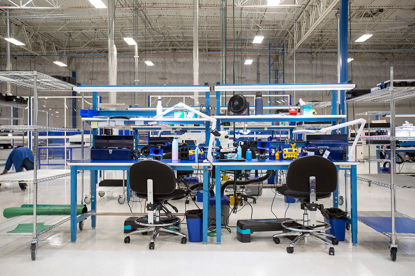
Modern electronics, especially portable devices, can have an astounding amount of circuit functionality. Communication, networking, navigating, photography, and various sensors are just some of the features of a handheld device. Electronic miniaturization for these devices isn’t possible without the benefits of high-density interconnect (HDI) printed circuit boards. Designers need an HDI PCBA manufacturer to successfully specify and build HDI-printed circuit boards.

Introduction →
| Features for HDI Designs | |||
|---|---|---|---|
| Microvia | Flex / rigid-flex | BGAs | High % SMD |
Shrunk via hole diameters significantly frees up routing with stacked/staggered layer transitions. |
Flex and rigid-flex boards allow greater space utilization within compact enclosures, replacing more intricate wire harnesses. |
The highest component pinout possible requires microvias and minimal trace widths for breakout. |
While SMD has a higher propensity for PCBAs, HDI box builds are likely to have an even greater restriction on component height. |
Exploring High-Density Interconnect PCBAs
A high-density circuit board provides many benefits to product designers, including circuit area reductions. Smaller circuitry generally improves performance by increasing functionality while reducing per-area power consumption. Here are some other benefits that product designers will realize by using HDI technology:
Key HDI PCBA Design Benefits:
A high-density circuit board provides many benefits to product designers, including circuit area reductions. Smaller circuitry generally improves performance by increasing functionality while reducing per-area power consumption. Here are some other benefits that product designers will realize by using HDI technology:
- Lower overall PCBA costs

- Increased circuitry density
- Better PCBA reliability
- Increased signal integrity and performance
- Decreased susceptibility to electromagnetic interference (EMI)
- Better thermal management
- Overall, improved efficiency in the design
One of the chief advantages of HDI technology in printed circuit board design is adding more functionality to the board through compression of the circuitry. There are several methods to accomplish this design compression:
- Newer components with smaller dimensions
- Smaller pin pitches, which reduce the space necessary for routing
- Tighter component packing
- Multiple via types in the design, including via-in-pad and microvia structures
- Use of smaller trace widths and spaces
- Thinner substrates support additional routing layers
HDI PCBA Manufacturer - DFM Requirements And Benefits
While time to market is critical, it can’t come at the expense of quality. Here at VSE, we excel in providing you both a quick turn on your circuit board builds and ensuring that they adhere to the highest levels of quality. Our PCBA manufacturing gives projects a pole position in developing new technologies:
High-density interconnect circuit boards require a carefully conceived board layer stackup configuration before the layout begins. This process will ensure the design’s impedance-controlled routing calculations are correct while optimizing signal integrity.
CAD systems can typically allow or disallow specific via types on certain nets or change spacing rules and trace width values. Design rules are essential in HDI design to avoid EMI and other potential signal integrity problems.
HDI designs use smaller trace widths and spacings that enhance the board’s routing density. Additional routing channels on inner layers also open up with vias that do not go entirely through the board. This configuration allows parts with high pin counts and low pin pitches to be routed on an HDI board. These blind and buried microvias can support or replace traditional through-hole drilling while offering significantly smaller drill diameters.