What is the PCB Fabrication Process?

A Successful PCB Assembly Starts with a High-Quality Bare Board Fabrication

EOL Components: How to Plan for Component Obsolescence

The manufacturing of a printed circuit board is a complex process that begins with a product concept and ends with a fully functional PCB assembly. Along the way a schematic is created to capture the net connectivity, the physical circuitry is laid out in a PCB design, and electronic components are ordered. After soldering the components onto the board and completing assembly testing and verification, the circuit board will be integrated into the full system.

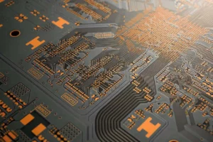
Taking a circuit board from start to finish has many intricate details that must be completed for success. One area in this process that doesn’t get the recognition it deserves is the fabrication of the bare board. The design of a PCB receives a lot of attention due to the complex software tools used in its creation. Manufacturing will get equally lauded in the satisfaction of completing the final product. But somewhere in the middle of this lies the mysterious process of circuit board fabrication, often unknown outside of the design world.
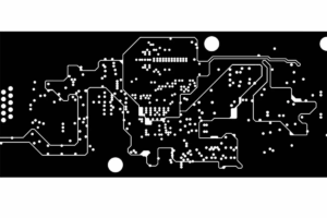
To uncover the tenebrous origins of a raw circuit board, and how it’s prepared for electronic components to be assembled to it, we will answer the question: what is the PCB fabrication process? To get truly acquainted, we will scrutinize what it takes to construct a high-quality circuit board fab that can be easily assembled by a contract manufacturer.

PCB Fabrication Basic Requirements

PCB fabrication is the process of building the raw board that will serve as the foundation for the final printed circuit board assembly. Before the fabrication vendor can proceed with the job of building the raw board, there is a checklist of design details that must be completed. Here are some of the items that must be accomplished to begin fabrication, and what data the board vendors will be looking for:

Circuit Board Details

Before beginning a PCB layout, the design team will work with their contract manufacturer to develop the parameters and configuration of the physical board. This information is necessary for the layout of the design, and for deciding on the PCB fabrication vendor best suited for the job. Some details will include:

Board layer stackup and configuration
Controlled impedance layers
Minimum trace width and spacing
Via types and structures
Copper balancing
PCB panelization considerations

Completed PCB Design

To ensure the accuracy of PCB manufacturing, the initial design must be complete. Even a simple component update that wasn’t synchronized between the schematic and the layout could result in a changed footprint and thus a bad board build. Here are some design items to check off first so the design is fully completed and ready for manufacturing:

  • Circuitry has gone through a full engineering review
  • Schematic and layout databases are updated and synchronized
  • All components are placed on the board, and all net connections are routed
  • Circuit simulation, signal integrity, and power integrity analysis are completed
  • PCB design rules and constraints are checked and errors corrected
  • Bill of materials (BOM) is reviewed for current and available components
  • Design for manufacturing (DFM) rules are reviewed for error-free assembly.

Full Manufacturing Design Data

With the design complete and ready to build, a full set of fabrication and assembly data files are generated and submitted to the contract manufacturer. The PCB CM will use these files to conduct their design reviews, and then forward them to the fabrication vendor to quote the build of the raw boards. These data files will include:

Gerber or other formatted board layer image files
Manufacturing drawings for fabrication and assembly
Bill of materials (BOM)
Component XY locations (pick & place)
Test point locations
Netlist
Schematic

With all checklist items completed and ready to go, the contract manufacturer can proceed with ordering the raw circuit boards needed for the assembly. Typically the PCB CM will have a list of preferred fabricators to work with and will choose the vendor whose capabilities best align with the technical requirements of the circuit board. Another factor in choosing the fabrication vendor is whether or not the board being built is a prototype. If so, the fabrication vendor must have the capabilities to run a separate production line outside of regular processes. They’ll also need to conduct their design reviews using the Gerber data being supplied by the PCB CM to maintain the highest quality in the prototype build.

Once the fabrication vendor has been chosen, the next step is to build the raw circuit board!

What is the PCB Fabrication Process to Build a Bare Board?

With all the necessary design information and data in hand, the PCB fabricator will begin building the raw board. Many types of circuit boards can be fabricated including single-sided boards, high-density multi-layer designs, and flex circuits. For this example, we will look at the basic steps required in the fabrication of a standard multi-layer circuit board.

Creating the Circuitry Images

The first step of circuit board fabrication is to transfer the PCB design circuitry image data from the manufacturing files supplied by the CM to the board. Usually, data arrives in a file format known as Gerber, although other formats and databases can be used. The image data will be transferred to the board by one of two different methods:

  • Photo Tooling: The standard imaging process in PCB fabrication that’s been in use for as long as circuit boards have been mass-produced. A precision photoplotter will create the circuitry images on film, which is used in the fabrication process as a template to print the images onto the board.
  • Direct imaging: A laser prints the circuitry images directly onto the circuit board bypassing the need for photo tools. This has advantages over using film because it’s more precise, there aren’t alignment issues, and photo tooling won’t require periodic recreation to replace worn-out films. Conversely, each layer will have to be laser printed individually, which is a more expensive process.

The Layers of a Circuit Board

A multilayer circuit board is a composite of different layers of dielectric material and metal conductors. It’s composed of layer pairs with a dielectric core material of epoxy resin and glass fiber more commonly known as FR-4, sandwiched between two layers of copper foil. While there are other dielectric materials available, FR-4 is the most common core material used in PCB fabrication.

Multilayer boards will take a thinner version of the same core structure used in the creation of a double-sided board, and laminate it together with other core structures to build the board layer stackup. Each layer must be strictly controlled for its width, copper weight, and layer to layer alignment for a quality final product.

Creating the Inner Layer Circuitry

The first step in PCB fabrication is to print circuitry images onto the inner layer cores:

  • The copper foil of the core is covered with a sheet of photoresist material.
  • The photoresist is exposed with either an ultraviolet light through the photo tooling or by direct imaging with a laser.
  • Only the areas of copper circuitry, such as pads and traces, are exposed which polymerizes, or hardens the photoresist over the circuitry patterns.
  • The unexposed photoresist, which is still pliable, is chemically removed from the copper.
  • The copper layers of the core are etched away leaving only those areas of circuitry that are protected by the polymerized photoresist.
  • The photoresist is stripped off leaving only the copper circuitry.

When this process is completed, the layers of the core will be inspected by an AOI system (automated optical inspection) for defects. Once each inner layer pair of the board has gone through this same process, they’ll be ready to be laminated into one complete circuit board.

Laminating the Layers Together

Together with thin layers of copper foil to cover the external surfaces of the top and bottom sides of the board, layer pairs are stacked to create a PCB “sandwich.” To facilitate the bonding of the layers, each layer pair will have a sheet of “prepreg” inserted between them. Prepreg is a fiberglass material impregnated with epoxy resin that will melt during the heat and pressure of the lamination process. As the prepreg cools, it will bond the layer pairs together.

Compositing the board together during this phase requires a lot of attention to detail to maintain the correct alignment of the circuitry on the different layers. Once the stackup is complete the sandwiched layers are laminated, and the heat and pressure of the lamination process will fuse the layers together into one circuit board.

Drilling the Holes

The next step in PCB fabrication is to drill holes in the board for component mounting, thru-hole vias, and the non-plated holes of mechanical features. The majority of the thru-holes used in a circuit board will be plated, and are usually drilled 0.005” larger than the specified finished hole size to allow for plating. If the design contains any blind and buried vias or laser-drilled microvias, those are fabricated before the lamination of the board. The extra process steps for these vias can add additional cost to the fabrication of the board but may be required for dense circuitry and/or electrical performance.

Once holes are drilled they get cleaned using chemical and mechanical processes to remove resin smears and debris caused by drilling. The entire exposed surface of the board, including the interior of the holes, is then chemically coated with a thin layer of copper. This creates a metallic base for electroplating additional copper into the holes and onto the surface in the next step.

Creating the Top and Bottom Layer Circuitry

Now the board is ready to have its top and bottom circuitry images printed. To do this, the same photoresist will be used as with the inner layers, but this time the circuitry needs to be unprotected and plated up with additional copper:

  • The top and bottom surfaces of the board are completely covered with a sheet of photoresist material, including the drilled holes to be plated.
  • The photoresist is exposed by UV or laser, but contrary to the inner layers, all surface areas of the board are exposed except for the circuitry patterns.
  • Once the unexposed photoresist is chemically cleaned off, the circuitry patterns of bare copper are electrically plated with more copper to build up their metal weight.
  • Next, tin is plated onto all of the copper circuitry as a protective layer, and the photoresist is stripped off the remainder of the board in preparation for etching.
  • The board is etched to remove all copper except for those areas of metal circuitry that are protected by the tin.
  • Finally, the tin is removed leaving the plated copper pads, traces, and thru-holes.

At this point the board’s circuitry is complete, but there are still a couple of more steps to finish the fabrication of the board.

Solder Mask, Silkscreen, and Surface Finishes

To protect the board during assembly, the solder mask material is applied using a UV exposure process similar to what was used with the photoresist. This solder mask will cover the entire surface of the board except for the metal pads and features that will be soldered. In addition to the solder mask, component reference designators and other board markings are silk-screened onto the board. Both the solder mask and the silkscreen ink get cured by baking the circuit board in an oven.

The circuit board will also have a surface finish applied to its exposed metal surfaces. This helps to protect the exposed metal, and assists in the soldering operation during assembly. One example of a surface finish is hot air solder leveling (HASL). The board is first coated with flux to prepare it for the solder and then dipped into a bath of molten solder. As the board is removed from the solder bath, a high-pressure blast of hot air removes excess solder from the holes and smooths the solder on the surface metal.

Assembly Prep, Inspection, and Test

The final step of the PCB fabrication process preparing the circuit board for assembly. If necessary the circuit boards are routed out of their manufacturing panels, or the panels are prepared for breakout after assembly. This is done by either scoring a V-cut on the board outline or routing out the board except for small breakout tabs.

The finished board goes through continuity testing with automated test equipment such as a bed of nails test fixture, or a flying probe test system. Tests look for any unintentional shorts between nets which would invalidate the board. Once the testing is complete and the board passes inspections, it’s shipped back to the PCB contract manufacturer for component assembly.

PCB Fabrication and Assembly, Working Together to Build Your Circuit Board

The successful manufacturing of a high-quality circuit board requires a seamless partnership with your PCB contract manufacturer and the fabrication vendor they choose to build the bare boards. To ensure the expected levels of fabrication quality, the PCB CM has a list of criteria that a fabrication vendor must pass to be considered as a qualified vendor. Here are some of the desirable attributes in a fabrication vendor:

  • They hold an ISO 9001 certification.
  • They are experienced in and have demonstrated proficiency with the type of PCB technology that is required.
  • They consistently deliver PCBs that measure up to the expected specifications and tolerances.
  • They can verify the design by providing cross-sections and a detailed first article inspection (FAI) report that measures all attributes of the board.
  • They are competitive on cost while achieving 100% on-time deliveries.

Local PCB contract manufacturers typically build a lot of quick-turn assemblies, so they need equally quick turn-around times on the bare boards that they order. They’ll want to cultivate partnerships with local PCB fabricators that respond quickly and have a reputation for building quality prototype boards. PCB CMs will also have overseas fabricators for larger orders that are more favorable on cost but less flexible on their delivery schedule.

VSE Understands Circuit Board Fabrication

Building you a superior circuit board is our goal at VSE. We understand the pressures you face in electronics markets, and we’re prepared to build your prototype, NPI, or production circuit boards on time, and at the highest levels of quality. To that end we have an advanced engineering team that is ready to help you on your project with the following:

  • Component sourcing and procurement.
  • Design engineering and PCB layout capabilities.
  • Bill of materials review with recommended alternatives.
  • Design for manufacturability review and recommended corrections.
  • Mechanical design with box build, wire harness, and cable assembly capabilities.

We also understand the importance of starting your PCB assembly with the highest quality bare board fabrications. We have an established group of PCB fabricators both locally and overseas to ensure we have the capacity for any project.

A Skilled and Experienced PCB Contract Manufacturer

We understand the PCB fabrication business because we have spent time working with many different vendors around the world. 35 years of experience working with a wide range of vendors has uniquely positioned us to help work through any concerns that you may have about the fabrication side of PCB manufacturing, and answer all of your questions. We have the knowledge and experience to get your next board manufactured. Give us a call and let us show you how we can partner to make your next PCB assembly a success.

Contact Us
reCAPTCHA