Electronic manufacturing services (EMS) are more than the boards delivered to clients at the end of production. By partnering closely with clients, VSE enhances product quality and the overall experience by managing every stage of the supply chain. Working with a domestic contract manufacturer (CM) means faster turnaround times, stronger responsiveness, and greater security than offshore options. With VSE, PCBA quality means products that meet specifications quickly, reliably, and securely, backed by exceptional customer service.

Integrated Quality From Start To Finish
We employ rigorous testing throughout production, including automated optical inspection (AOI), in-circuit testing (ICT), X-ray inspection, functional testing, and burn-in. This layered approach confirms reliability, safeguards performance, and reduces risk across every build.
For example, when a medical device startup brought us an early prototype, our layered testing caught a power stability issue before production — avoiding weeks of redesign and thousands in delays.
By combining design validation, process monitoring, and end-to-end testing, VSE delivers products that consistently perform to the highest industry standards.
Proven Processes That Drive PCBA Quality
Quality Management System (QMS)
Pre-Production Design Review
Trusted Vendor Sourcing
Certifications That Back Our Commitment
VSE is committed to serving our clients, as demonstrated by the industry-recognized certifications that back our robust quality control (QC) measures. Per ISO 9001, we’re continually refining our manufacturing practices to provide better performance, reliability, and complexity for our clients’ designs. Whatever your EMS needs, VSE ensures your build quality is as exemplary as its design.

Protecting Documentation And Intellectual Property
VSE employs strict documentation control practices, covering version control, revision management, and secure data transfer, to prevent costly delays and protect sensitive design data. This ensures the right version is always in the right hands, protecting your IP and your schedule.
Beyond documentation, we prioritize intellectual property and national security. Our domestic manufacturing model, ISO-driven processes, and facility safeguards ensure that confidential designs and hardware remain protected from counterfeiting, reverse engineering, or theft. Every client engagement is treated with the same high level of confidentiality and protection.
Assembly Is At The Heart Of Our Quality Electronic Manufacturing Services
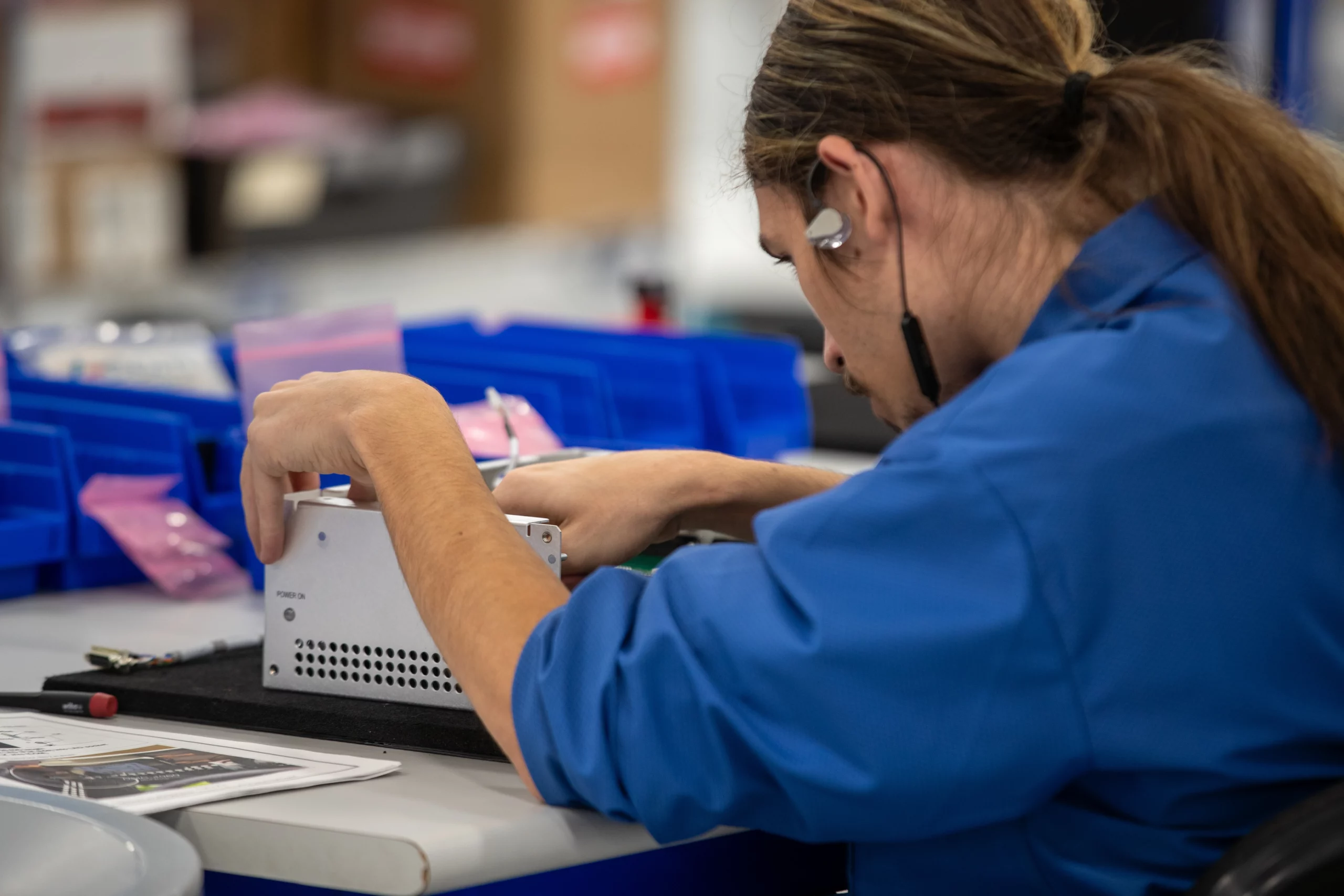
From components to casing, VSE ensures every part of your product is aligned, tested, and built for real-world reliability.
We can enact ECOs and revisions without additional input from our customers. We balance high quality and reliability against cost and manufacturing complexity to maintain rapid turnaround times.
Component sourcing has become more critical than ever, with long lead times and shortages. We examine every BOM for obsolescence and end-of-life (EoL) production status before leveraging multiple vendors for sourcing redundancy. Our procurement team works behind the scenes to identify alternative components and prevent production delays, so your engineering team can stay focused on innovation, not chasing supply chain issues.
From flex/rigid-flex to high-density interconnect (HDI) placement, our team of engineers and technicians is committed to translating your documentation into a product. Moreover, we’re committed to understanding your market and end-users and fully delivering on design intent.
Maintaining reliability in electronic systems is paramount for several industries and applications. Yet, as much attention as the soundness of the PCBA receives, a suitable enclosure will go a long way to preventing damage and poor conditions that can reduce a product’s service life.
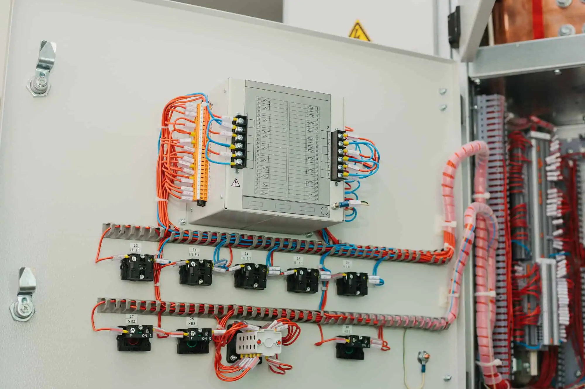
As electronic systems grow more complex, so do their testing regimens and intra-board connections. A well-organized wire harness aids in testing and troubleshooting while maintaining the mechanical integrity of connectors.

Partnering For Smarter, Stronger EMS Solutions
Moreover, we see our clients as partners and fully engage with the design to understand the industry, market, and end-users for potential design-for-manufacturing (DFM) adjustments. Whether you’re designing in tightly regulated spaces like medical technology, need precision standards for the semiconductor industry, or want to lean on the experience of a domestic CM with a proven record of realizing our clients’ life-saving and life-changing technology, VSE is here to assist you.
Quality-First Production, Backed By Experience
If you are looking for a CM that prides itself on its care and attention to detail to ensure that each PCB assembly is built to the highest standards, look no further than VSE. Contact us today to learn more about partnering with us for your next project.