Manufacturing a printed circuit board is a complicated process. From fabrication through assembly, there are many different points during manufacturing that must be verified before the board can pass to the next step. This validation can be done in several ways, from manual inspections to advanced X-ray analysis.
Another standard validation method is the different automated optical inspection (AOI) systems used to examine PCBs. The use of AOI equipment in PCB manufacturing will often generate a lot of questions, including the following:
- What is automated optical inspection?
- How does an AOI system work?
- For what manufacturing processes is it used?
- How is AOI incorporated into PCB production?
- What are some of the key benefits of using AOI?
Let’s look into these questions in greater detail to find out how automated optical inspection used for PCB manufacturing validation can help you end up with a better circuit board.
Some Common Questions About Using Automated Optical Inspection in PCB Manufacturing
Automated optical inspection equipment is used in different ways during PCB manufacturing to verify the various production processes. Scanning the board automatically frees up operators from having to examine all of the minute details on each board. Instead, the operators can focus on the system’s defects, resulting in a more efficient and reliable inspection process. AOI systems have been in use for some time, but many are unfamiliar with it and have the following questions:
What is it?
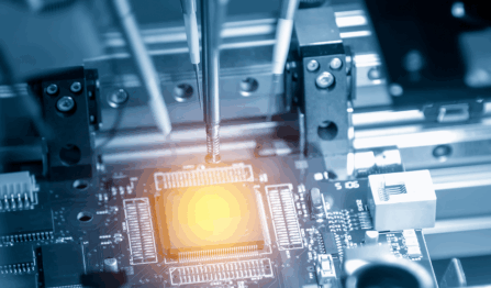
AOI systems capture an array of images using high-resolution cameras with LED illumination sources for automated comparison or laser scanners with micron resolution in the X, Y, and Z axes. The type of inspections being conducted determines which system is used. For instance, solder paste inspection equipment will use laser scanning to determine the volume of solder on a pad, while assembly verification systems focus on the images of solder components.
How does it work?
A first article printed circuit board is manually inspected. Once confirmed as being good, it will be run through the AOI system to establish it as the “golden” unit for future comparisons. For assembly verification, the AOI will “learn” from the golden unit what good solder joints look like and the correct component values, locations, and orientations on the board. With this information collected in its database, the system will then compare the images of new boards scanned and alert the operators if there are any inconsistencies. These systems can also be “tuned” to recognize and allow acceptable alternate parts as well.
What does it inspect?
AOI systems inspect the various phases of printed circuit board manufacturing, both during fabrication and assembly.
Fabrication:
- Shorts between the copper of different nets.
- Trace width violations.
- Spacing violations between traces, pads, vias, and fills.
- Cuts in the copper would result in an open or disconnected net.
- Excess copper on a net.
- Missing component footprint pads.
- Drilled hole breakouts in PCB pads or vias.
Assembly:
- Solder paste inspection before assembly.
- Finished solder joints.
- The alignment of components on a board.
- Polarity indicators for component orientation.
- Component markings such as color bands on resistors.
- The correct location of targeting fiducials.
- Labels and other circuit board markings.
How is it used?
AOI systems are used primarily to validate the manufacturing processes being used to construct a printed circuit board. When a board is fabricated, the AOI systems will verify that the board has been built according to its specifications. This verification is essential for parameters such as controlled impedance routing, where the trace widths must hold a specific tolerance for signal integrity purposes. For PCB assembly, the AOI systems will verify that the designated components are installed, positioned, and soldered correctly.
What are some of its key benefits?
Manufacturers use automated optical inspection equipment to verify the circuit boards they are building with a high degree of reliability. These systems check the entire board and compare it to the standard that has already been programmed into it much faster than standard inspection methods. The AOI systems used for assembly verification will also detect some counterfeit components with non-standard markings or colors.
Automated Inspections Help Build Better Printed Circuit Board Assemblies
A circuit board can have hundreds of components with thousands of pins connected with several hundred individual nets. Trying to reliably examine each of those thousands of points on every circuit board assembly that is manufactured is too much for visual inspection. Like looking for a needle in a haystack, It creates inspection fatigue and exceeds the limits of human attention for even the most diligent of rework technicians.
On the other hand, using AOI systems in circuit board manufacturing will find fabrication or assembly errors and report their findings back to the operators. With this information, the rework technicians can focus their attention on correcting any problems. AOI systems have established a more reliable inspection process that can handle a higher workload than what’s possible with standard inspection techniques.
At VSE, we use our AOI systems to verify our PCB assembly processes to ensure the best quality in the circuit boards that we manufacture for our customers. We understand the value of using advanced technologies like this in PCB assembly, and our technical staff has the skill and experience needed to get the best results.


