 Stories about detectives that can spot clues in a crime scene that others miss are really fascinating to me. Whether it is turning the pages of a Sherlock Holmes mystery or watching a rerun of “Monk,” I love to see these investigators find important details that no one else can. But even the greatest of these detectives would be hard-pressed to spot problems on a printed circuit board being assembled. On a complicated board, there could be thousands and thousands of opportunities for a defect to exist, and manual inspection simply can’t reliably search through all of them in a reasonable amount of time.
Fortunately, there is an invaluable piece of equipment that should be in use at your PCB assembly house that is designed to help. As part of the different methods of inspection that your contract manufacturer should use, the automated optical inspection (AOI) system is what will handle the majority of the inspection on your PCBA. This system can quickly evaluate the thousands of details that are too small for the human eye to catch and report any detected problems back to the operator.
To quote Sherlock Holmes: “It has long been an axiom of mine that the little things are infinitely the most important.” That is certainly true when inspecting PCBAs. Let’s take a closer look at the AOI PCB system and how it helps your CM to produce a better circuit board for you.
AOI for PCBs is a critical inspection method for a quality circuit board assembly.
What Is AOI PCB Assembly Inspection, and How Does it Work?
Automated optical inspection equipment has been around for a while now, and it is constantly being enhanced and updated to improve its capabilities. This style of inspection equipment is used in many industries, including PCB manufacturing, where it is used for inspecting bare boards, solder paste application, and assembly. For PCB assembly, the AOI system inspects the placement and soldering of components and will alert inspection technicians to a variety of potential problems, from incorrect parts being used to bad solder connections.
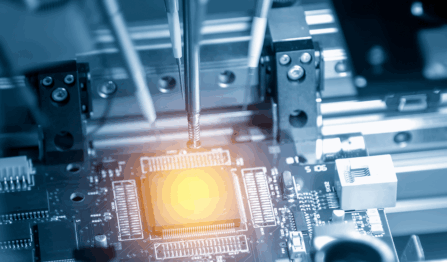
AOI PCB inspection equipment relies on a system of high-resolution cameras as well as different sources of illumination, such as fluorescent, LED, ultraviolet, and infrared, to capture an array of images. These images are processed by the system, which is programmed to examine different details of the assembled board, including:
- Solder joints
- Component alignment
- Polarity indicators
- Resistor color bands
- Markings
- Fiducials
- Labels
When a new PCB is assembled, the contract manufacturer will run the board through the AOI system after the parts have been placed, and then again after the board has been soldered. The multiple images captured during these processes are used to develop a “golden” standard for what the board should look like after a successful assembly.
On subsequent runs, the AOI system will scan each assembled board and compare those images to the images of the golden standard board it has on file. When it finds areas that it can’t reconcile with its golden standard, it will flag those areas as possible defects for the technicians to examine in more detail. The technicians can then use the system to bring up a detailed close-up view of the problem for their examination.
AOI Tunability: The Key to Successfully Preventing Assembly Defects
The PCB AOI equipment can be “tuned” as needed for the board being assembled. For instance, an alternate part could be flagged as a defect because its markings and shape didn’t match the golden standard. The AOI operators, however, can make adjustments to the programming to accept that specific alternate part so that it isn’t flagged in the future. The more boards that are run through the system, the more it learns what to look for as the operators fine-tune the programming from the additional assembled images.
The tunability of the system allows contract manufacturers to filter out those issues that are acceptable and to catch hard-to-see defects that used to be extremely difficult to find by visual examination. The manual inspection process required the technicians to look at each part, marking, and solder joint on the board, which could range into thousands of details to examine on complex boards. With so many details to examine, it is easy to understand how imperfections could be missed.
The AOI system, on the other hand, allows highly skilled inspectors to be able to focus solely on the relatively few potential defects identified by the system. This gives your CM the upper hand on finding actual defects in a relatively short amount of time compared to the more labor-intensive manual inspection process.
What Can You Expect From Your CM Regarding AOI Inspection?
AOI inspection systems have revolutionized the PCB manufacturing industry. As boards have become more complex due to the higher-density placement of smaller components, manual inspection can no longer be relied on to catch assembly defects.
You can no longer afford to have your boards manually inspected, and you should insist on automated optical inspection. The time you will spend in debug trying to find a small solder bridge or an incorrect part number is simply not worth what it will cost you.
At VSE, we have a wide variety of testing and inspection methods that we regularly use on all of the boards we manufacture, including AOI. Our technicians are highly experienced in using these systems, and our AOI equipment is a critical component of our PCB assembly operation. From incoming inspection of raw materials and parts to the functional testing of the assembled board under power, we ensure your board is assembled and operating the way you intended. Our goal is to deliver the best possible assembled printed circuit board back to you.
