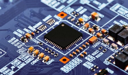
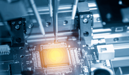
 There is a lot that goes into the manufacturing of a printed circuit board assembly. From start to finish, there are many processes involving different levels of machinery, automation, and human intervention. Like a well-rehearsed stage production, all of these processes work smoothly together toward the completion of the finished circuit board. While all of these processes are vital, there is one that doesn’t have as high of a profile as the others—the PCB inspection process.
Inspection is often relegated to the role of a bit player in a room full of divas. With their endless activity, the pick-and-place machines live a glamorous life, while the solder systems live an exciting one of dangerously hot molten solder. PCB inspection, on the other hand, doesn’t typically share that same spotlight, and its importance in manufacturing is often overlooked or downplayed.
Don’t believe it though—high-level precision inspection techniques are essential to the successful manufacturing of your PCBA. The right components must be placed on the board correctly, and their solder joints must be verified to be solid. Without processes performed by your contract manufacturer to ensure critical printed circuit board inspection criteria are met, you wouldn’t have the assurance that your board was built to the highest levels of quality, and premature or intermittent circuit board failures would be commonplace.
The 3 Most Critical PCB Inspection Criteria
Printed circuit board assembly inspections are primarily focused on verifying the correct placement and soldering of electronic components on PCBs. To do this, three main PCB inspection processes should be used by your contract manufacturer:
- Automated solder paste inspection (SPI): Working from the same CAD files used to make the solder application stencils, SPI systems use a laser scanner and high-resolution image processing to inspect solder paste shape, volume, and alignment to the pad on the board. The amount of solder paste on a pad can vary depending on the component to be attached, and the shape of the solder can be different than the pad on which it is applied to reduce solder voids or bridges. Manual inspection of solder paste like this is ineffective. However, automated systems can tell operators if the solder on the board is adequate, and even if the solder application equipment needs cleaning or changing. With small high-density parts like ball grid arrays (BGA) that hide solder joints from automated optical inspection systems, fully effective SPI is essential.
- First article manual inspection: After attaching components to the first circuit board, an inspector will check all of the parts against the bill of materials (BOM) before the board goes through the solder reflow process. The inspector will confirm that the components match the BOM and that their location and rotation is correct so as to provide a known “golden” board for the automated optical inspection process. This board is then passed through the automated optical inspection system to establish a “golden” set of images that the rest of the manufactured boards will be compared to automatically.
- Automated optical inspection (AOI): Using the known “golden” first article board as the standard, the AOI system will compare components for correct placement as well as all visible solder joints on subsequently manufactured boards. This system uses a combination of illumination wavelengths and high-resolution cameras to check part markings, such as polarity indicators and resistor color bands. It will detect open solder joints, insufficient solder, solder bridges, and misaligned parts.
The system can also be tuned depending on the needs of the boards being processed. Alerts of false defects can be tuned out while certain anomalies can be made more sensitive to alert the operator to critical areas. The AOI system can also be programmed to accept alternate parts as well.
These are the three main inspection processes and their criteria that a PCBA will go through, but there are some additional steps that can and should be included as well.
Additional Inspection Processes for Complete Process Control
For those boards with a greater level of complexity in their component placement, there are other inspection techniques that your contract manufacturer should use in addition to the three main processes listed above.
The first is an X-ray examination of the board. 2D X-ray systems are used to inspect components, such as BGAs and quad flat no-leads, for alignment and solder defects. There are also automated 3D systems that can be used, depending on the needs of the board.
Another inspection method is an endoscopic system optimized for inspection of BGA solder joints. It uses a very small prism at the tip, which can be moved around the entire perimeter of a BGA to inspect for optimal and uniform solder joints.
Your CM will also have a very detailed inspection process for incoming components and materials used in the manufacturing of your PCBA. These processes will be tuned to the type of component, its materials, the supplier, and its history to verify the accuracy of the incoming components. On the other end of manufacturing, your CM will also have a process in place to ensure that all of the products to be shipped out completely pass their final quality inspection criteria.
The Level of Inspection You Should Expect From Your CM
All of the PCB inspection processes and systems listed above should be in use at your CM in one form or another. They should be checking incoming components and materials, manually and automatically checking your board during assembly, and then verifying the final product before shipping it back to you.
At VSE, we have the experience and equipment you need for the best inspection processes in the industry. We also optimize our inspection processes and systems for prototype builds, pilot builds, new product introductions, and small-to-medium manufacturing so that you receive the most benefit for your specific builds. Our inspection processes, combined with our test capabilities and our goal to test as much as possible within your constraints, maximize the opportunity to find and correct potential defects before your PCBAs are shipped back to you. You can see the results of this effort reflected in our very low defect rate.
