Home > Blog
FEATURED BLOGS →
PCBA Enclosure Design Guidelines
This article discusses some primary considerations impacting PCB enclosure design.
Learn More
Home > Blog
FEATURED BLOGS →
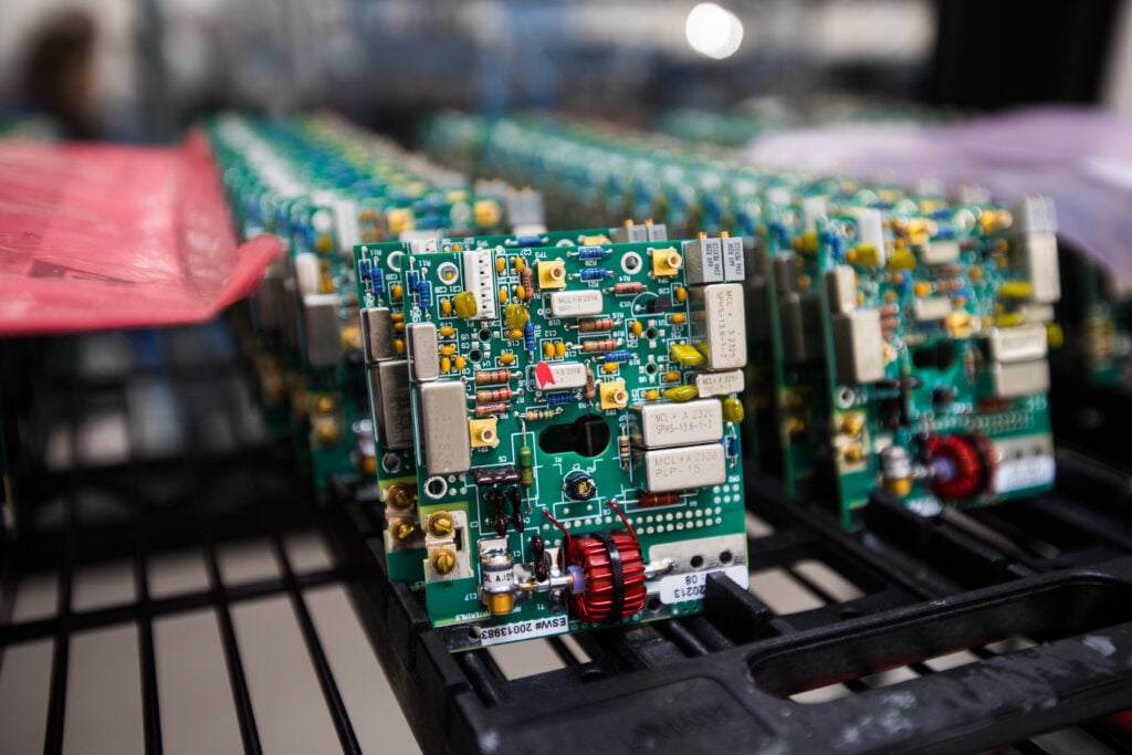
Supply Chain Management in the Electronics Industry
supply chain management, engineering team, test department, design prototype department, executive team, materials management, quality and compliance department
Learn More
Home > Blog
FEATURED BLOGS →
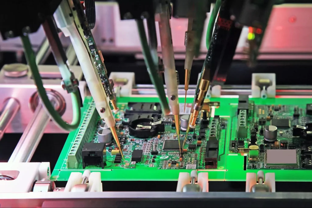
PCBA Reliability Testing: Quality and Efficiency
Electronics are only as valuable as their uptime, as scheduled or (especially) unscheduled maintenance can significantly hamper business operations or end-user satisfaction. However, the nature…
Learn More
Home > Blog
FEATURED BLOGS →
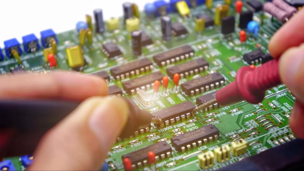
PCB Test Point Guide for Successful Design
PCBs require test points to be strategically designed into the board, along with components and routing the connections. Bare board continuity testing, in-circuit testing,…
Learn MoreOur Blog
Blog
Supply Chain Management in the Electronics Industry
4 Min. To Read
supply chain management, engineering team, test department, design prototype department, executive team, materials management, quality and compliance department
Blog
PCBA Reliability Testing: Quality and Efficiency
6 Min. To Read
Electronics are only as valuable as their uptime, as scheduled or (especially) unscheduled maintenance can significantly hamper business operations or...
Blog
PCB Test Point Guide for Successful Design
7 Min. To Read
PCBs require test points to be strategically designed into the board, along with components and routing the connections. Bare...
Blog
Navigating And Managing PCB Production Costs in 2025
8 Min. To Read
The landscape of PCB manufacturing is shifting, and designers need to adapt their supply and manufacturing chains to stay competitive....
Blog
Semiconductor Industry Forecast 2025
14 Min. To Read
The 2025 semiconductor market outlook with segment forecasts, regional analysis, and emerging technology trends shaping industry growth.
Blog
PCB Assembly BOM Best Practices for Low-Volume Builds
9 Min. To Read
Here are some of the best practices for your PCB assembly BOM to help streamline component management and optimize your...
Search
Popular Blog Post