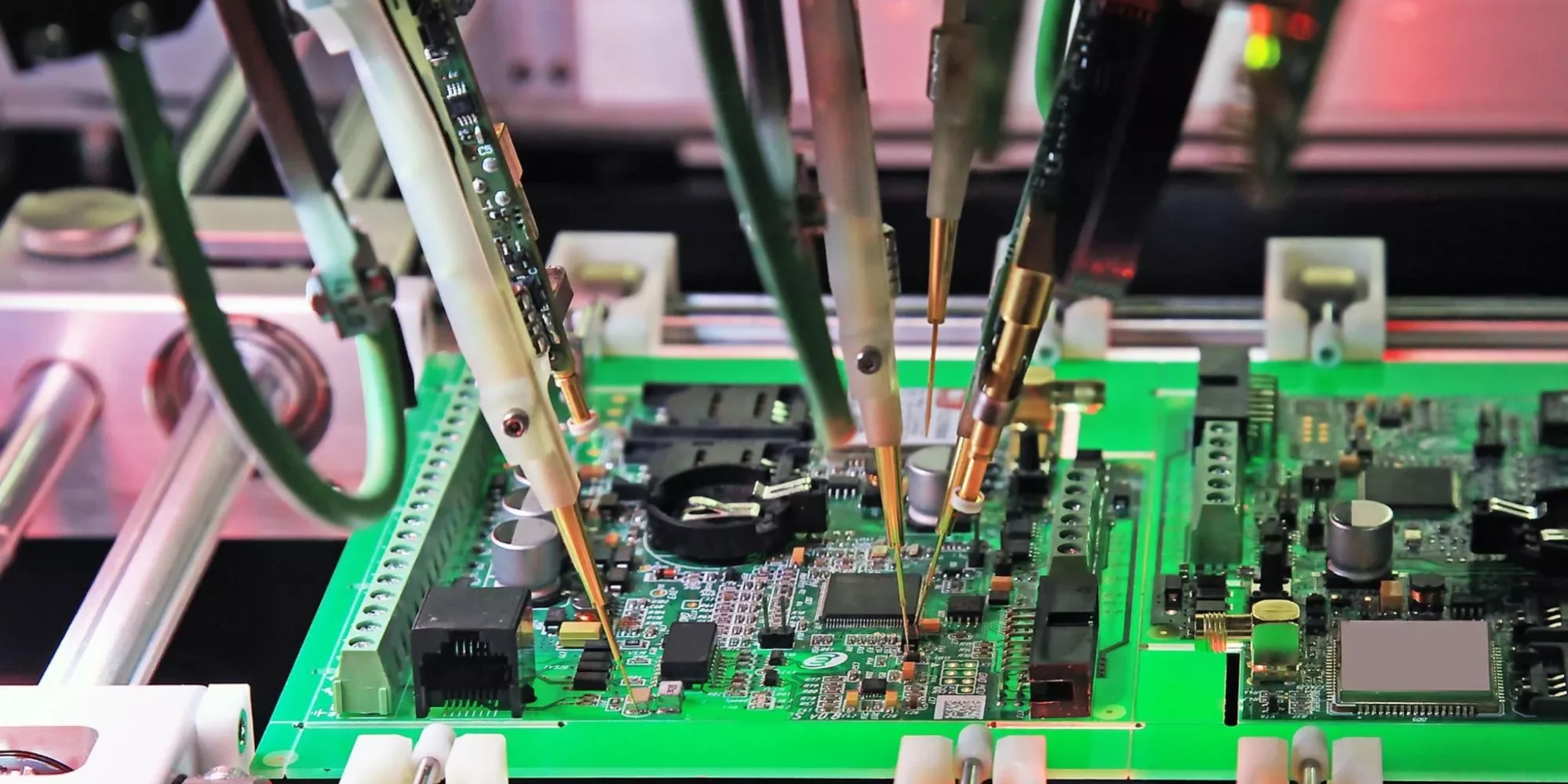
PCBs require test points to be strategically designed into the board, along with components and routing the connections. Bare board continuity testing, in-circuit testing, and flying probe testing all require the presence of test points on the board to facilitate their processes. Follow our PCB test point guide below to understand how to build a fully testable circuit board.
Printed Circuit Board Test Points
![]()
There are two different types of “test points” used in a PCB design. The first is a small metal contact, or test point, connected to a net. This test point can be an existing thru-hole lead, via, or a specifically placed metal pad, and one test point is usually assigned to each net on the board.
Once assigned, the PCB CAD system will use their XY locations and net assignments to generate data files for the automated test systems. These systems conduct either continuity testing for shorts during PCB fabrication or solder connectivity and functional testing during circuit board assembly. Two types of machines are usually used for this testing:
- In-circuit test (ICT) or “bed-of-nails”: These test machines use a fixture designed and built for each board in production. The fixture contains spring-loaded probes that simultaneously contact each test point on the board, allowing for all nets to be tested simultaneously. These machines conduct their tests very quickly, but the fixtures are expensive and time-consuming to design, build, alter, and maintain.
- Flying probe: These test machines feature three to six probes that move around the board and conduct their tests. Without the need to design and build a test fixture, the flying probe is an inexpensive machine to use. However, due to the individual nature of its testing, the flying probe is a much slower process and is usually reserved for limited production runs and prototypes.
The second “test point” to define is the specific points on the board accessible to technicians doing manual testing and repair. Usually, these are referred to as probe points. The following chart points out the differences between test points and probe points:
| Test point – automated testing | Probe point – manual testing |
| Smaller size contact pad | Larger size pad for thru-hole post or loop |
| Can be a via, existing thru-hole, or new pad | Only a pad specified for the post or loop |
| Is not marked on the board | Will have a ref des, and a net name |
| Can be spaced closely together | Needs spacing for technician access |
With the nature of test points now clearly defined, let’s look next at some layout strategies for placing PCB test points to help the testability of the circuit board.
PCB Test Point Guide: Layout Strategies
Here are some PCB test point guide recommendations for defining and placing test points on a circuit board. However, since manufacturers differ in their capabilities, the designer must verify these parameters before committing to them in their design.
| Topic | Details |
| 1. Test point sizes and shapes |
|
| 2. Test point to test point spacing |
|
| 3. Test point to component spacing |
|
| 4. Test point to board edge spacing |
|
| 5. Test point placement |
|
| 6. Probe point parameters |
|
| 7. Probe point identification |
|
PCB Testpoints Guide: Where to Place Test Points and Implement Them
Determining where to place test points is a balance between test coverage, accessibility, and manufacturability. Here’s a step-by-step practical approach:
1. Identify Critical Nets and Coverage
- Ensure all power rails, ground, and key signal nets are accessible for testing.
- Include test points on high-risk nets, such as those with fine-pitch components or critical routing, to catch opens and shorts during testing.
2. Leverage CAD Tools for Automation
- Use your PCB CAD system’s auto test point generation to place test points efficiently on unrouted or untested nets, then review placement for accessibility and clearance.
- Adjust shape (square/round) and size as per your fixture and probe type, referencing your design rule constraints.
3. Consider Probe and Fixture Access
- Position test points on the solder side of the board if using ICT; avoid shadowing under large components.
- For manual probing, place probe points on the accessible side with clear silkscreen marking and net identification for technicians.
- Ensure sufficient spacing from components and edges for test probes, as well as consistent distribution to avoid board flex during testing.
4. Align with Inspection Strategy
- Keep test points clear of areas critical for AOI and X-ray inspections to prevent false positives and imaging artifacts.
- Use tented vias or appropriate solder masking to reduce the risk of solder bridging while maintaining electrical contact for probing.
5. Document Test Points Clearly
- Maintain a test point map and table showing net names, XY positions, and test point types (automated vs. probe points) for your test engineering and manufacturing teams.
- Include test point data in your fabrication and assembly outputs (ODB++, IPC-2581, or CSV files for test fixture design).
Visual and Automated Optical Inspection (AOI) Considerations for Test Point Design
In addition to supporting electrical testing, test point design should facilitate effective inspection during fabrication and assembly. Automated Optical Inspection (AOI) systems scan the board for solder defects, misalignments, and surface anomalies. To support AOI:
- Maintain a clear solder mask definition around test points to improve contrast for AOI cameras.
- Avoid placing test points under components unless necessary; exposed test points are easier to inspect for solder bridging or cleanliness.
- Ensure test points have consistent, defined shapes (e.g., round or square) to avoid false flags during inspection.
- If using fiducials near dense test point areas, ensure they are not confused with test points by maintaining different sizes or a clear silkscreen indicator.
X-Ray Inspection and Test Point Placement
X-ray inspection (AXI) is often used on boards with BGA or bottom-terminated components, where direct visual inspection is impossible. For test points:
- Avoid placing test points directly under dense BGAs, as they can shadow the area during X-ray inspection.
- Keep test point vias tented in X-ray critical regions unless they are explicitly used for testing, to avoid confusing inspection images.
- Distribute test points in a way that allows X-ray visibility of solder joints, avoiding creating unnecessary layers that block critical inspection paths.
- For boards requiring both X-ray inspection and ICT, align the test point and pad design so X-ray images remain interpretable while maintaining testability.
Final Inspection Readiness and Cleaning Access
After testing, boards often undergo a final visual or manual inspection and cleaning process:
- Allow probe clearance for cleaning tools by spacing test points away from sensitive components where cleaning fluid may accumulate.
- Use silkscreen markers or reference designators for critical probe points so manual inspectors can easily locate and verify connections.
- Design test points to withstand post-test cleaning without lifting or damaging solder joints, using robust pad design and controlled solder volumes.
Automated Testing at Your PCB Contract Manufacturer
By following this PCB test point guide, you will ensure that your automated test points and manual probe points effectively ensure the manufacturability of your printed circuit board. At VSE, we have been configuring circuit boards for full testability for over 40 years, and we can help you with your questions about automated PCB testing.
If you are looking for a CM with the engineering and testing expertise to ensure that your PCB assembly is built to the highest standards, look no further than VSE. Contact us today to learn more about partnering with us for your next project.


