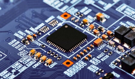
High-density pinout components using a package-on-package (PoP) construction, most notably ball grid arrays (BGAs), feature pitch (pin-to-pin distances) much smaller than historical standards. Given their proliferation in modern electronics due to their broad functionality, designers and manufacturers have had to adapt processes to accommodate the tighter pitches. Fine-pitch PCB design focuses on how layout and fabrication can minimize performance issues with these constraints in mind.
Starting With the Stackup
PoPs are self-contained circuitry combining discrete memory and processor boards into a component stack. This arrangement has significant space savings (at the cost of greater protruding height from the board) that endear it to small form factors where the board area is at a premium. Incorporating these fine-pitch components impacts a majority of the design rules and stackup. Advantageously, some fine-pitch PCB stackups can sidestep the extra fabrication costs of via-in-pad (which optimizes available placement and routing space). Consider the following stackup:
| Comparing Potential Fine-Pitch PCB Stackups | |||
|---|---|---|---|
| Layer | Good | Better | Best |
| 1 | Signal (Top) | Signal (Top) | Ground |
| 2 | Signal | Ground | Signal (high speed) |
| 3 | Ground | Signal (high speed) | Signal (high speed) |
| 4 | Power | Signal (high speed) | Power |
| 5 | Signal | Power | Ground |
| 6 | Signal (Bottom) | Signal (Bottom) | Signal (Bottom) |
The Good stackup provides extensive routing layers. However, layers 1/2 and 5/6 can suffer from crosstalk that imperils electromagnetic compatibility (EMC), as no reference layer separates the back-to-back signal layers. Additionally, controlled impedance calculations can swing wildly without an adjacent reference plane. Note that impedance increases as the height from the reference plane increases; therefore, fabricators may have to shrink the trace width to accommodate the correct targeted impedance. This factor can increase cost/decrease yield if the fabricator is already operating at the extent of their capabilities.
The Better stackup contains an identical signal layer count as the Good stackup but with a more mindful approach to signal integrity. By placing the high-speed signal layers back-to-back at the center of the stackup, both signal layers have a neighboring reference plane, and they can have identical dielectric constants on either side of the trace (surface-level traces contend with atmospheric dielectric constant on one side). However, there are a few drawbacks: routing high-speed signals on inner layers necessitates a via transition from the top or bottom side assembly unless using a costly embedded assembly. These via transitions can complicate timing and length matching without careful consideration. For multi-power net boards, designers must avoid routing over split planes at all costs, as traces referencing multiple reference planes drive electromagnetic interference (EMI).
The Best stackup may initially seem confusing, as it trades a coveted routing layer for an additional ground layer. Fine-pitch PCBs rely on every mil of routable board area to accommodate high-density interconnect (HDI) assemblies, so how can designers afford to give one away? Consider that the most populous net in a design is almost universally ground – even with distinct ground nets, a design is unlikely to have more than 2 or 3 grounds (analog ground, digital ground, chassis ground, etc.). Placing ground on the top layer eliminates a significant amount of vias to ground, which increases the routable area on layers 2, 3, and 6. This method is most effective in single-sided or double-sided assemblies where the bulk component placement occurs on the top side.
Fine-Pitch PCB Design Rules
The design rules will require considerable changes to meet the tighter routing requirements of a board containing fine-pitch components. The biggest change will be defining pads as non-solder masks; typically, board pads are solder-mask-defined. Non-solder mask-defined (NSMD) pads have:
- Tighter copper dimensions; these dimensions produce smaller pads that assist in routing dense interconnects
- Reduced stress on the solder joint compared to solder mask-defined pads that improve assembly reliability.
However, NSMD pads may suffer worse adhesion and lower peel strength due to reduced surface area between the copper pad and fiberglass/epoxy laminate. Some additional rules to consider:
- Provided pad sizes remain below 10 mils, a trace width of ~3.25 mils can fit between the pads on the mounting layer with a ~3.25 mils clearance to neighboring pads on either side. Mounting-side layer routing greatly assists with breakout and can remove many vias. With the above clearance constraint, designers can place dogbone vias (if not using via in pad) at the center of any four neighboring vias (i.e., half the vertical pitch, half the horizontal pitch). Designers can then route those signals on internal layers or the opposite side of the board.
- Teardrops added to pads on the corresponding routing layer improve the mechanical strength of the pads and assembly.
- Avoid oversized traces (this is a common practice for power/ground nets to support a low-impedance pathway), as the small size of BGA pads requires even heating for proper assembly. Do not tie multiple same-net pads with a copper pour without adding thermal reliefs.
- A 0.5 mm pitch supports a 5-mil hole/10-mil pad via using the via placement described above.
Your Contract Manufacturer Has an Eye for HDI
Fine-pitch PCBs reflect the various challenges of HDI designs for board fabrication and assembly. While most manufacturers can handle the complexities of HDI manufacturing, getting design and manufacturing on the same page as soon as possible leads to quicker turnaround times and fewer revisions. Here at VSE, our engineers are well-equipped to handle the challenges of translating HDI designs to physical boards. Our engineers are committed to building electronics for our customers, including a thorough design review process that balances design intent and manufacturability. We’ve been realizing life-changing and life-saving devices alongside our valued manufacturing partners for over forty years.


