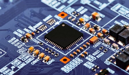
During the testing stage, if you discover issues like unwanted signals interfering with the device’s operation, components consuming more power, or overheating, there is likely some error in design. The late-stage discovery of these errors can mean an irreplaceable impact on manufacturing cost, product quality, and device performance. Given the critical importance of precision in the design stage, PCB designers tend to take the design for manufacturability (DFM) approach.
DFM strategy is highly effective in identifying PCB layout issues, thus optimizing the fabrication and assembly process to be more efficient and reliable. Let us explore this DFM approach to understand how to design a PCB.
How To Design a PCB: Taking A Design For Manufacturability Approach
In the continually evolving process of PCB design, the manufacturing process should focus on more than just the design. Cost and quality are equally important to maintain your competitiveness. The DFM approach focuses on quick, efficient, and cost-effective manufacturing of PCB.
The DFM techniques are practices used to optimize the PCB design process, making it more streamlined. These practices include anything from circuit connection and PCB layout information to cost control. DFM checks are a manufacturer’s go-to for keeping the assembly and fabrication on track and looking out for potential design issues. Here’s what makes the DFM checks important:
- Focusing on the board’s functionality is important, but DFM also analyzes the manufacturing capabilities and limitations of the design. Oftentimes, the designs are not optimized for the component placement phase. This means making additional adjustments during assembly leading to an increase in manufacturing cost. DFM eliminates the need to redesign and rework the product, reducing the associated cost.
- With DFM checks, you can optimize aspects such as trace width, electrical connections, layer stack-up, stiffener incorporation, etc. The optimized design reduces the likelihood of defects during production and enhances the device’s performance.
- DFM enables optimization of PCB design for testability. Including test points, fixtures, and self-test circuits, makes it easier to test the device for any problems and identify their potential solution.
- Clear DFM guidelines help reduce the design’s complexity. This is an advantage for product quality and improved productivity, resulting in less cost and time in high-volume production. This result is because the clarity in design leads to fewer defects, eliminating the need for repairs for a low-cost and timely assembly.
The check for functioning and manufacturability in PCB design with DFM guidelines is a key to improving quality and reducing turnaround time.
DFM Analysis Steps In PCB Design
Although there aren’t any defined DFM steps on how to design a PCB, it is important to look into the details in each phase of assembly and manufacturing.
The following are some basic DFM verifications to make for compliance:
| Design and Layout Specification Check | Review of design specifications is important to ensure they align with the performance and cost expectations. This part of the DFM analysis will ensure that there aren’t any PCB design and layout issues, and commencing the production will result in the product without any physical or electrical errors. The step includes a check for trace width, layer count and thickness, vias, copper fill, silkscreen, and stiffener design. Evaluation of placement and clearance between parts are also important to avoid errors later in the process. |
| Material Compliance | DFM analysis for material compliance includes a check for the metallurgical and thermal properties of the material, i.e., if it can effectively handle the heat and electricity while performing the intended. The material must comply with standards such as RoHS (Restriction of Hazardous Substances ) and WEEE (Waste Electrical and Electronic Equipment). |
| Manufacturing Compliance | Compliance is essential for selection and optimizing the manufacturing process. This part of the DFM analysis should focus on product size, material in use, and accommodation for the desired production limit. |
| Testing | This stage of DFM analysis focuses on examining the functionality and quality of the prototype and individual components to determine if it meets all the requirements and is ready for high-volume manufacturing. |
One major advantage of using the DFM guidelines is its ability to identify issues such as acid traps and solder masks which may go unnoticed with regular visual inspection and impact the circuit board performance. The DFM approach to PCB design is an opportunity to define limitations and optimize manufacturing capability.
Optimize Your PCB Design Process
How can you design a PCB efficiently? This question has guided designers towards techniques such as DFM, improving PCB design’s technical and production aspects. DFM aims to enhance quality, productivity, and cost-effectiveness by identifying, mitigating, and optimizing the design issues in the preliminary phase.
Here at VSE, alongside our manufacturing partners, we help you identify the DFM issues and walk you through the optimization best practices. Therefore your PCB design results align with the desired specification and high-quality standards you’ve come to expect.
If you are looking for a CM that will collaborate with you in understanding how to design a PCB and ensure the assembly is built to meet the highest standards, look no further than VSE. Contact us today to learn more and to get started on your next project.


