I used to check my physics equations by hand in college, despite powerful solvers available to me with a few clicks and keystrokes. It may have been an appreciation for the process work or plain stubbornness. Either way, whenever my solution didn’t match the author’s, I needed to know that my errors weren’t conceptual or algebraic. Overall, I prefer diagnosing how and why problems arise to gain confidence in my understanding before switching to automated approaches.
This manner of working is fine for self-enrichment but does not endear itself to throughput due to its combined limitations of speed and accuracy. While manual PCB testers are still an extremely valuable resource, high-volume lots become more manageable with increased automated PCB testing.
The Present Technology of Automated PCB Testing
![]()
Automation is not some far-off possibility; many current processes have specialty test equipment that can accurately gauge the presence of some desirable feature (or absence of defect) in a much shorter amount of time than human operators.
The keys to any automated tester are repeatability and scalability:
- Repeatability ensures that from the time a device under test (DUT) begins evaluation, it is subjected to an algorithm that proceeds stepwise until a final determination can be made. Support for this system should include some internal troubleshooting mechanisms to detect issues with the test mechanism and sort borderline cases.
- Scalability indicates that test equipment can handle the volume expected of large production lots without a meaningful drop in performance. Depending on the equipment or process methodology, false positives and negatives will be encountered at some rate, though at levels far below human operators for the test volume.
One of the hurdles to fully automated testing is the lack of modularity. A particular tool will only test for one parameter and potentially with only a single analysis pathway. While these tools are exceedingly complex and sophisticated, they are limited by their specificity. For manufacturers, this equates to a need for multiple pieces of equipment with their learning curves and servicing schedules. It is not only the test equipment that lacks modularity – this can also extend to test fixtures, such as the case for a bed-of-nails tester.
While this is a worthwhile time investment on a significantly large production lot, test points at the design level and fixture fabrication need to be incorporated into the manufacturing schedule at an early stage of development to prevent unnecessary delays.
Semi-automated testing cycles are also worthy of mention. JTAG/boundary-scan exists parallel to the electromechanical probe-based testers. By combining the board netlist with a boundary scan description language (BSDL) file, JTAG testers can automatically create tests to check for logic and memory errors in the design or manufacturing defects like opens and shorts. JTAG does require space to implement at the board level (this is an advantageous trade, provided the density of the design does not preclude it) and may be unsupported at the IC level. Ultimately, boundary scan provides an additional diagnostic tool in support of more fundamental in-circuit tester (ICT) units.
The Future of Automated PCB Testing
AI presents an interesting complement to automated PCB testing. One of the drawbacks of current tests is the need for human oversight: some results can’t be easily siloed without a deeper level of intuition. Like most devices, no matter how sophisticated, there is a need for interpretation beyond the scope of the machine’s capabilities.
AI learning solutions like convolutional neural networks (CNN) offer one potential route for intelligent decision-making without human intervention. These models take data input over a guided training period and discernment by analyzing features of an image – a simple sample would be a CNN that learns to distinguish cats from dogs. More pertinent to PCB manufacturing would be the ability to detect defects (poor solder reflow, voids, missing components, etc.) to filter boards without additional supervision.
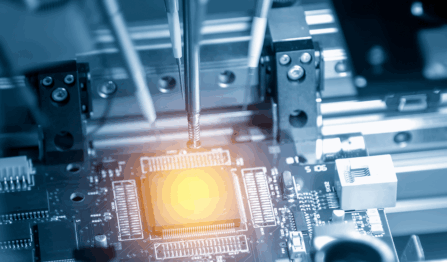
This manner of automation is already in use today, though the implementation is imperfect. Both automated optical inspection (AOI) and automated x-ray inspection (AXI) can capture images (images otherwise imperceptible in the case of AXI) and meet some of the criteria set out above for automated testing. Furthermore, both methods do not require any particular interfacing between boards and the testing unit, making their applicability universal without any additional inclusions by the designer.
While these methods can quickly identify and parse certain defects, they may struggle with others. AOI provides only a 2D image that lacks depth and restricts perspective, and 3D-image solutions offered by AXI significantly reduce throughput. Even with the best possible image, the sheer variety of potential defects makes automated AI sorting a difficult proposition, not to mention the defects an image cannot detect.
Like most technology applications, there exists a middle ground. Improvements to AI further the autonomy of the technology, which may continue to require human management, but will improve testing outcomes, reducing overall defect escape.
Your Contract Manufacturer’s Commitment to Quality is Automatic
Automated PCB testing has yet to take the form of full automation, and it’s uncertain if it will ever be fully automated. Still, improvements in computer vision offer manufacturers an additional tool to save time and money on defect analysis. This tool provides immediate yield benefits for the manufacturer and commensurate savings for clients while sharpening revisions and later productions as a feedback mechanism. Testing, whether manual, automated or somewhere in-between, requires a dedicated group that is as well-trained as it is well-equipped. VSE’s team of engineers is motivated in building electronics for customers with excellence and reliability as guiding principles. Alongside our professional manufacturing partners, we aim to deliver nothing less than optimum performance for your devices.


