On a recent cross-country flight to visit relatives, our plane was grounded due to a defect in one of its weather sensor systems. That day’s weather was spectacular, and I’m sure there was no need for this system. However, since a functional sensor was on the go/no-go decision list, we were grounded until the fault could be repaired. Airlines have definite rules governing detecting defects like this to ensure their passengers’ safety.
As with any manufactured object, circuit boards can also be plagued with unexpected defects. OEMs can trace PCB defects back to many causes, which is why it is so important to detect these problems early on before they become unmanageable. Fortunately, there are many methods available to designers and manufacturers for PCB defect detection, and we will look at some of these methods here.
Potential Defects in Printed Circuit Boards
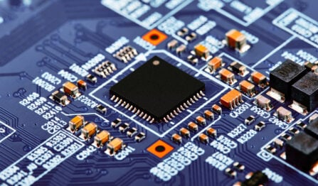
PCB defects can originate from many sources, ranging from how a board was built to the components used on it. Here are some of the more common defects to be aware of:
- Fabrication errors: If a board is fabricated incorrectly, it can lead to nets that are shorted together or nets that are not entirely connected and are “open.” Poor fabrication methods can degrade a metal trace causing it to be etched too much, reducing its strength, and creating signal integrity problems by changing its impedance.
- Component problems: If incorrect parts are specified in the bill of materials, or the parts are compromised in their ability to operate, the board may also experience failures.
- Assembly defects: Poor assembly methods can lead to many different PCB defects. These problems include solder not forming correctly in plated thru-holes, nets being shorted together by excessive solder, parts not getting enough solder for a good connection, or small surface mount devices getting miss-aligned during assembly.
These general categories of PCB problems can be manifested in many different ways, and they must be found and corrected to produce a good quality circuit board. Next, we’ll look at some of the methods used by designers and manufacturers for PCB defect detection.
PCB Defects Detection Methods
Circuit simulation
Simulation Programs with Integrated Circuit Emphasis systems, or “SPICE” tools, are used to validate the performance of the circuits in a PCB before the board is built. This simulation can save time and expense on building multiple prototype boards for testing and find hidden problems that could surface later as a PCB defect.
Design rule checking
Design rule checking (DRC) features are included in CAD systems to check the schematic and the PCB layout. The rules and constraints entered into the DRC system will check the design while it is being worked on or run in a batch mode at any point in the design cycle to review the entire database. One example of a DRC is reporting metal from different nets that are too close to each other, which could short together during the manufacturing process.
Signal analysis tools
Another useful step in the PCB design process is to analyze the signal and power nets of the layout for performance. These systems will report different signal and power integrity problems with the board that could affect or interrupt its operation.
3D modeling
The ability to view the PCB layout in 3D gives designers a better picture of how their placed components interact. With 3D, designers can spot potential conflicts between components that may not have been obvious with the standard 2D view. 3D modeling also helps when board layouts are combined with mechanical designs to see how all circuit boards will fit together in the full system.
Automated optical inspection
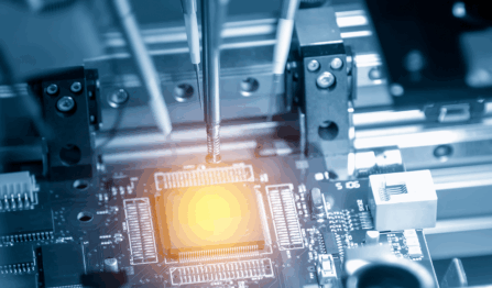
AOI systems are used throughout the printed circuit board manufacturing process to verify PCB fabrication, solder paste application, parts placement, and final assembly. These automated optical systems can detect defects in the following categories:
- Fabrication integrity
- Part numbers
- Component polarities
- Part alignment and rotation
- Solder joints
By automatically scanning a circuit board and comparing those scans with stored images of a correct example, the AOI system can flag potential irregularities that a technician will confirm. This process takes hours off a traditional manual inspection and is much more accurate. In some cases, X-ray systems are used to examine elements that are difficult to inspect visually, such as solder joints hidden by parts or other obstructions.
Automated testing
Circuit boards are tested automatically after manufacturing for net continuity, assembly verification, and component functionality. These test systems use different configurations of probes to contact test points designed into the boards to conduct the tests. Technicians can also do testing manually but at a much slower rate.
Inspection
Even with all of the automation, many PCB defects are detected through standard human inspection techniques:
- Incoming parts and materials are inspected.
- Inspection stations are set up to monitor process steps during manufacturing.
- The board goes through a final inspection before being packaged and shipped to the customer.
How Your PCB Contract Manufacturer Can Help
At VSE, we are well aware of the importance of PCB defect detection throughout the design and manufacturing flow. Starting with our engineering department, we can offer circuit design and PCB layout expertise to find potential problems and correct them before building your project.
We also closely work with our PCB fabrication vendors and vet their capabilities to create the highest quality bare board fabs possible. When it comes time to assemble your circuit board at VSE, you can count on the following in our production facilities:
- Multiple automated and manual inspection points throughout the manufacturing process.
- Automated testing to verify assembly and functionality.
- Precision manufacturing processes are fine-tuned for accuracy.
- Industry-wide reputation for quality in circuit board manufacturing.


