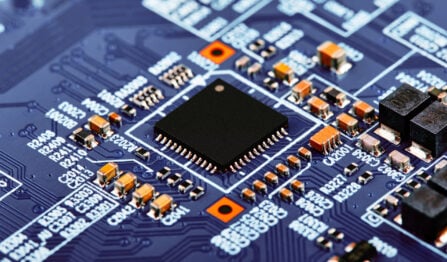
The power delivery network (PDN) of a circuit board provides both power and ground to the design, and connecting the components to the PDN is one of the standard steps in PCB layout. But as signal speeds have increased, PCB PDNs have demanded more care and attention in their configuration, especially the ground plane. For good signal integrity, it is essential to lay out the design so the ground plane can provide clear return paths for digital, analog, and mixed-signal designs.
Through the years, there have been many attempts to enhance circuit board signal integrity by altering the ground planes, but that often isn’t the best solution. This article will look at the problems with different ground plane configurations and some of the better alternatives. We will also list some recommendations to help with the layout of PCB grounding in mixed-signal designs.
The Question of Whether to Use Separate Ground Planes in Mixed-Signal Designs
As signal speeds rose on mixed-signal circuit boards, engineers experimented with different steps to improve the signal integrity in the designs. One problem was the tendency for signal return paths in the ground plane of either digital or analog circuitry to create crosstalk in the nearby routing of the other type. To resolve this problem, designers tried splitting the ground plane into separate analog and digital planes. The thinking was that the split would solve the noise problem by isolating the circuitry into two different areas. However, it resulted in more interference problems instead.
Isolating digital and analog ground into separate planes may be helpful for designs where those areas of circuitry are entirely isolated and don’t have any interaction with each other. It may also be necessary for safety if your design generates high-voltage currents from an isolated power supply. But for a standard mixed-signal design, splitting a ground plane into separate analog and digital sections can introduce new electromagnetic interference (EMI) problems.
The ground plane in a circuit board should provide clear return paths for the signals in the design. If high-speed signals are routed over an area of the board that doesn’t have a ground plane adjacent to it, they will be forced to find an alternate path back to their source. Whatever alternate paths the signal returns finally use may have a large loop inductance acting like an antenna radiating EMI and ruining the signal integrity of the design. Analog signals routed across voids in the ground plane can also exhibit similar EMI problems.
Effective PCB Grounding in Mixed-Signal Design
The key to eliminating the signal integrity problems caused by EMI is to design an effective ground plane into your circuit board’s PDN. The ground plane must be able to support clear signal return paths for:
- Digital circuits
- Analog circuits
- Mixed-signal digital and analog circuits that connect
| Designers should avoid using split ground planes in mixed-signal boards where digital and analog circuitry interact for the best signal integrity. |
The best grounding to use in a mixed-signal printed circuit board design is a complete and continuous internal ground plane. PCB designers should partition the placement of the components on the board to avoid the problems of crosstalk caused by digital and analog circuitry encroaching on each other. Carefully partitioning the design into separate sections will give the needed isolation of analog and digital components. With the speed of digital signals today, their return paths on the ground plane will stay close to their trace routing on the adjacent signal layer. The tight coupling of the return path to the signal trace routing allows designers to plan their design with clear signal paths.
Even on circuit boards with unusual shapes or areas of the ground plane broken up with slots or other features, you can still make the single continuous ground plane work. The important thing is to ensure that you don’t route over any obstructed ground plane areas, providing a clear signal return path. Here are some other layout ideas that can help you meet your PCB grounding expectations for mixed-signal designs.
Layout Tips and Recommendations for Mixed-Signal Ground Planes
For a successful grounding system in your mixed-signal PCB design, here are some layout recommendations:
- Partition your component placement to keep a separation between digital and analog circuitry.
- Instead of routing ground with traces, use a continuous plane to avoid splits, cuts, or other features that obstruct the signal return paths.
- Do not route analog traces through digital circuitry or digital traces through analog circuitry.
- Keep power supply components separate from the analog and digital circuitry, and do not route analog or digital traces through the power supply circuitry.
- The most important recommendation of all: do NOT route high-speed traces through areas of the ground plane that are obstructed with cutouts or other features of the board outline.
Remember that your PCB contract manufacturer can help with additional tips and recommendations for creating a robust PDN that will serve the needs of your mixed-signal design. At VSE, we’ve been helping our customers with questions and concerns about their designs for over 30 years. Our engineering staff is ready to help you with your mixed-signal designs too.


