 Long before the cell phone and the internet, many relied on the good old citizens’ band radio, or “CB,” for our social media. Being voice only, it was more restrictive, but it was also kind of charming to just talk to folks through the radio—until my neighbor down the street powered up. Running much more power than what the FCC allowed, his interference dominated the local frequencies, and you wouldn’t be able to get a word in edgewise until he shut down.
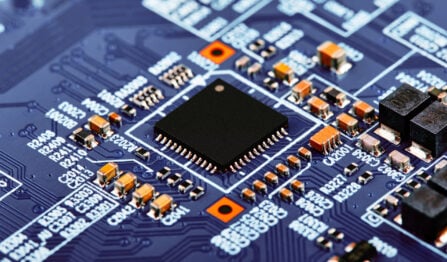
Interestingly, after all of these years, I can still remember how annoying that interference was, which is why I have a lot of respect for the electromagnetic interference, or EMI, on a PCB. A circuit board can be the recipient of EMI unless preventative measures are taken in its design. The PCB you design can also create EMI with other electronics if you don’t take the same precautions. This article will look at some of these precautions and how to avoid electromagnetic interference in PCB designs.
The Challenges Created by EMI

The general effects of electromagnetic interference between electronic devices are noticeable. Wireless communication systems are interrupted by unexpected broadcasts, automotive systems may malfunction, and advanced sensors used in medical or other applications may not transmit the complete or correct data. Some entertainment venues will combat this by requesting that wireless devices be deactivated during a performance. Flight attendants still make a similar request before the takeoff and landing of commercial flights. Even back in CB radios’ days, we learned to avoid revving our cars’ engines to reduce the engine noise from our transmissions. But EMI prevention goes much further than that, and there are many different design standards in place to specify how much interference is or isn’t allowed:
- IEC 60601-1-2 is a series of standards that define medical equipment’s essential performance and safety expectations when confronted with EMI.
- CISPR 12 is a regulatory requirement to ensure that automobiles’ internal combustion engines do not interfere with wireless communication when the vehicle is near residences or businesses.
- CISPR 25 ensures the performance of radios and other communication equipment mounted in vehicles equipped with internal combustion engines.
However, the issues with EMI go a lot deeper than how radio is affected in a car or whether or not a wireless microphone picks up a stray signal from another source. Within the circuit board itself, EMI can disrupt how the board works. Computer systems rely on the clear transmission of their data and memory signals between processor and memory devices and on and off the board to those external system ports where they are connected. Interference here can create a lot of background noise, raising the ground reference level, which can cause a signal to be misinterpreted at the wrong state. Interference like this can create intermittent issues or outright failures of the system. Next, we’ll look at what causes some of these EMI challenges on a printed circuit board.
EMI Causes
While there can be many different sources of EMI on a circuit board, here are some of the main ones to be aware of:
- Simultaneous switching noise (SSN): The circuits on the PCB are constantly switching as the connected devices perform their functions, and this activity can create noise that is radiated as EMI. When many of the outputs on a large CPU or memory device all switch simultaneously, and in the same direction, the simultaneous effect is much worse.
- Antennas: A large metal area on the circuit board can behave as an antenna and radiate EMI. These areas can include metal plane layers on the board, tall components, heat sinks, and even the system chassis where the board is mounted.
- Return paths: When high-speed transmission lines are not paired with an adequate reference plane for the signal to return on, the returning signal will wander around the board until it finds its way back to the source. This lack of a clear return path can create a lot of EMI on the board.
- Crosstalk: This occurs when unintentional electromagnetic coupling occurs between traces on the circuit board routed too close together. The louder or aggressor signal will overpower a weaker signal, which then mimics the aggressor’s behavior instead of doing what it is supposed to do. The same issue can happen between traces on adjacent layers of the PCB if the traces are routed in the same direction. Here it is referred to as broadside coupling.
EMI Prevention
To prevent these scenarios from happening, consider implementing the following design techniques on the board:
- Layer stackups: Make sure to use the proper layers and stackup configuration for your design. While fewer layers may reduce the board’s manufacturing costs, they may cause some of the challenges listed above. Your board will need adequate reference planes for clear signal return paths and a well-designed power delivery network to filter out the switching noises.
- Component placement: Good signal and power integrity start with the proper placement of the components on the board. Sensitive nets that could potentially create noise need to be kept as short as possible, depending on how close their components are to each other. The same goes for high-speed transmission lines as well as power supplies. Simultaneously, enough room must be left between the components to get all of the trace routing completed. Be sure to place plenty of bypass capacitors as close as possible to large CPU and memory devices to absorb their power spikes.
- Trace routing: Much of the trace routing will be guided by how well the components are placed, but there are some points to remember here as well. Keep high-speed transmission lines and controlled impedance lines on layers to use direct reference planes for signal return paths and shielding in a microstrip or stripline configuration. Be careful with split planes or other obstructions that might block the clear return paths on a reference plane. Keep routing as short and direct as possible except when traces have to be routed to a specific length. For power supplies, keep the traces as wide as possible and avoid right-angle corners in your routing.
Many other PCB design methods can help control EMI on your circuit board, and here is where you can find more information on those.
Additional Help on How to Avoid Electromagnetic Interference
The PCB contract manufacturer that will be building your board can usually give you a lot of help to control EMI on your circuit board design. For instance, one of the most important methods of preventing EMI on a circuit board is choosing the best configuration of the board layer stackup. The PCB CM will have plenty of experience building different circuit boards, and they will know the best layer stackup plan for your design.
At VSE, we have been working with customers like you to build precision circuit boards for over 30 years. Our engineering team understands the electrical and manufacturing requirements that must be met to build each design successfully. This expertise gives them the ability to advise you on the right layer configuration necessary for the best signal integrity performance and many other design measures to keep EMI under control.
If you are looking for a CM with the engineering capabilities to ensure that each PCB assembly is built to the highest standards, look no further than VSE. Contact us today to learn more about partnering with us for your next project.


