I recently added some additional security cameras around my house. We haven’t had any problems in my neighborhood, nor do I have any reason to believe that there will be any in the future. The technology is inexpensive, easy to install user-friendly, so it made sense to use it to my benefit. Knowing that the cameras will automatically detect and record any unauthorized activity on our property gives everyone some extra peace of mind.
When a printed circuit board is built, it’s also beneficial to have added assurance, except in that case we’re looking for problems in manufacturing. Not that we expect to find any defects, but we want to ensure that if a problem does come up we can find and correct it efficiently. This PCB defect detection process takes place with both the bare boards after they are fabricated and the fully assembled circuit boards, both of which we will examine in greater detail below.
Finding Defects in Fabricated Printed Circuit Boards
The circuit board fabrication process laminates layers with metal traces and planes on it together with dielectric layers for insulation in-between. Holes are next drilled for either component pins to be inserted or to connect metal traces from one layer to another. PCB fabrication is an exacting manufacturing process with tight tolerances, and the slightest error could result in the metal of one net coming into contact with another.
To ensure that none of the circuits on the board are shorted together, the board will be tested to verify its electrical continuity.
Testing these raw fabricated boards is done with either a bed of nails test fixture or a flying probe test system. Using the net connectivity data from the CAD tools used to design the circuit board, the test systems will go through each net to verify that they do not come in contact with any other net on the board. Usually, the fabricator will test the first circuit boards off the production line to establish a “gold” unit. If these first article tests do not detect any defects, then the entire production run will be considered as having passed their connectivity testing.
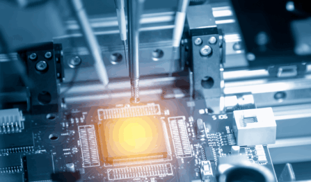
In addition to the automated testing, a bare board fab will also be visually inspected with a combination of manual and automated inspection techniques. Automated optical inspection, or AOI, will scan the board and compare the images with the images from the golden first article production boards. This equipment will then flag any errors it detects to the technicians running the scans. Additionally, the boards will be inspected by technicians trained to find errors that the automated systems might miss. Once the boards have passed their tests and inspections, they’ll be ready for the next phase of manufacturing, which is PCB assembly.
PCB Defect Detection of Printed Circuit Board Assemblies
Printed circuit board assembly is the process of installing electronic components onto the raw fabricated circuit boards, and then soldering them into place. This is done through a variety of techniques including solder reflow ovens, wave solder, selective solder, and of course, manual hand soldering. Like PCB fabrication, the assembly processes must also conform to tight tolerances to prevent errors like solder shorts, incomplete solder joints, and tombstoning. To verify that the assembly process has been completed successfully, the manufacturer will use similar PCB defect detection techniques as the fabricator:
- Visual inspection: The PCB contract manufacturer’s staff of experienced technicians will inspect the boards for assembly errors, which are often corrected through manual rework.
- Automated inspection: Not only are the AOI systems used to verify the fabrication process, but they also work well in finding assembly errors. With a known golden PCB for comparison, the AOI system will scan each board checking component values, rotations, and solder joints.
- Flying probe testing: Testers use between two and six probes to automatically move around the PCB and make contact with designated test points on the board. They are the same type of testers used for fabrication, but here they test for signals coming from the assembled components verifying their soldered connections. Flying probes are quick to set up and easy to run, but are limited with only a few probes to test all the different nets on the board.
- In-circuit testing: Like a flying probe, the ICT system tests each net to verify that each component is securely soldered to the board. The difference is that the ICT system is a bed-of-nails test fixture, testing all the nets on the board at once. This makes for a very fast test, but building and configuring the fixture is a long and expensive process.
- Functional testing: Manufacturers will also test the board for its electrical functionality. While this can be done in a limited capacity with flying probe testing, the ICT system can contact all test points at once and is thus preferable. There are other systems available for full functional tests, including cable scan and regular bench tests by a technician.
The goal of the manufacturing inspection and testing is to find there are no defects, which can be helped by following precise PCB design rules.
Avoiding PCB Defects by Following Good Design Principles
Many errors detected during inspections are influenced by how the circuit board is designed for manufacturability (DFM). Shorts are sometimes the result of not obeying metal and components to board edge clearance rules. Solder defects can be tracked down to the pad and/or hole sizes in the board, or even how the solder mask or solder paste features are configured. Tombstoning is a result of thermal imbalances due to one of the pins being flooded with metal and acting as a heat sink.
To avoid problems like these it is important to set up and use the rules and constraints within your PCB design CAD tools. To get the correct clearance values for these rules, it’s best to partner with a PCB contract manufacturer that has proven design engineering experience. At VSE we have been working together with our clients for over 30 years. We manufacture circuit boards with reduced assembly errors through adherence to good DFM rules and processes.
If you are looking for a CM that can help you design your board for error-free manufacturing at the highest standards, look no further than VSE. Contact us today to learn more about partnering with us for your next project.


