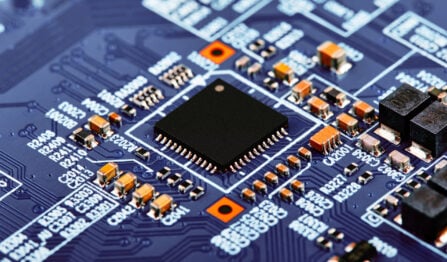
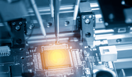
Accomplishing the levels of technical performance in modern electronics requires an incredible amount of sophistication in designing high-speed electronics. Methods once reserved for advanced printed circuit board design have now become the standard. High-speed design is in everyday items, from consumer cell phones to industrial and medical technology, that improves users’ quality of life tremendously.
The optimum performance of today’s PCB designs relies on effective placement and routing schemes for high-speed circuitry. A poor or careless layout harms the integrity of the signal paths and may ultimately degrade the overall performance of the circuit board. To ward against these issues, PCB designers must know the best signal integrity practices during layout. Robust design will also extend to regular signal integrity testing to ensure manufactured circuit boards work as intended.
Scoping Common Signal Integrity Issues |
||
| Oscilloscope reading | Design fault | Correction |
| Edge aberrations on waveforms. | Improper terminating resistance/impedance, semiconductor/switching element quality. | Check impedance matching and isolate + test switches to observe the response. |
| Reduced amplitude, secondary periodicity in waveform amplitude. | Reflections | Check for stubs in layout, and consider back drilling for vias in high-speed designs. |
| Significant noise on the ground. | Ground bounce | Reduce leakage current and check resistance in power supply and return paths. |
| Noticeable waveform when trace should not be active. | Crosstalk | Proper clearance, avoid running single-ended traces in parallel over long distances. Especially high-speed/noisy lines may need shielding. |
| Variations in periodicity of signal (i.e., clock). | Jitter | Keep clock traces as short and direct as possible, and avoid routing near (both in-plane and layer-to-layer) noisy, high-speed, or fast-switching signals. |
The Value of Signal Integrity Testing
To ascertain the peak operating performance of a printed circuit board design, design teams need to check for any signal integrity issues that need correction before entering production. A contract manufacturer can conduct PCB testing on the board after manufacturing. However, signal integrity problems found at that point are only mitigable at best, depending on the source and location.
The best thing is to design for the optimum signal performance possible from the outset. Developing in this fashion means working with a contract manufacturer to plan out the board’s materials as well as the configuration of the layer stackup. Dynamic simulation and analysis of the design will also help to enforce the best high-speed design layout principles.
Even if a board isn’t running at speeds that would typically qualify it as a high-speed design, there are a couple of general design aspects to consider:
- As a board evolves throughout its lifecycle, newer parts running at higher speeds can replace older ones. A design that didn’t necessitate high-speed best practices in early iterations may reverse course later.
- A design may introduce signal integrity issues into other system-level boards through cables or system interconnects. Designers need to account for the design needs of an individual board and its interaction with other boards in the electrical system.
Signal Integrity Problems That Can Affect PCB Performance
Form follows function, and choices made for fabrication and assembly during design layout can seriously impact signal integrity. Consider some of the foremost design issues that could impact board performance:
- Speed: High-speed circuits must consider board materials, board layer stackup configurations, component placement, and routing topology.
- Grounding methodology: Impedance-controlled traces need stripline or microstrip routing configurations for optimum performance. The current return path requires ground planes to be directly adjacent to the layers of the routed signals, careful selection of board materials, and practical layer stackup configurations.
- Split ground planes: High-speed signals need a continuous return path on an adjacent ground plane layer. A typical signal integrity error is when the return plane splits for power or ground redistribution. Although this solves the power network problems, there needs to be a return path to create a lot of noise for those high-speed circuits. Additional signal noise can create false signals triggering the circuitry to fail.
- Signal technology: Different types of signal technologies, such as analog, digital, ECL, or others, will require different approaches to routing. At the board level, these signal technologies will account for trace widths, spacing, and which board layers to route on. The wrong approach to routing these circuits could introduce problems to the board.
- Analog/digital noise sensitivity: Areas of different design technologies also need to be isolated. Sensitive high-speed transmission signals routed through noisy analog circuitry could cause performance problems in those signals.
- RF noise sensitivity: Areas of RF circuitry are susceptible to other circuitry and, in return, can interfere with surrounding circuitry. Isolate RF circuits with ground planes, stitching vias, and, in some cases, physical shielding.
- Sensitive components: Other components, such as high-gain amplifiers, may also have special sensitivity needs. These devices may require voids in power and ground planes to isolate them from other circuitry.
All of these potential signal integrity problems, along with other characteristics, can impact the board’s performance. Rectifying performance issues can introduce additional costs if fabrication material changes are required or if the board needs to be manufacturable as-is and requires a complete redesign.
How an Experienced CM Can Help You With Signal Integrity Concerns
Your contract manufacturer can help design a high-speed printed circuit board. When you work with an experienced CM, they have years of experience building high-speed circuit boards and are very qualified.
By reviewing your design, they will understand your overall performance goals and interface requirements and be best positioned to help you. With their experience, they can recommend board layer materials and layer stack-up configurations that will best fit the needs of your PCB. They will also devise the correct testing processes to verify the functionality of your high-speed circuitry, and they can even help guide you if you need help with signal integrity testing.
At VSE, we start working on your project by conducting a thorough design review. Reviewing the layout gives a complete picture of what we must do to successfully manufacture and test your board. We can advise you on high-speed design techniques and recommend board materials and layer configurations to give you the high-speed signal performance you’re looking for.
We can handle any PCB layout or circuit changes needed to enhance the overall signal integrity quality and performance, or we can help you to find external signal integrity analysis services if that is your preference. By leveraging our technical base and experience, you can minimize your PCB manufacturing time and iterations and ensure that design intent is reflected in the final product.


