
The landscape of PCB manufacturing is shifting, and designers need to adapt their supply and manufacturing chains to stay competitive. While the global trade environment is in flux, one strategy remains constant: finding or strengthening a relationship with an experienced contract manufacturer (CM) who can navigate supply chain complexities. At VSE, our commitment to partnership ensures a customized, high-level approach to solving your design challenges, which can accelerate turnaround times and help you meet critical time-to-market deadlines. We are a trusted, U.S.-based electronics manufacturing partner offering custom, high-quality PCBA solutions.
Key PCB Cost Drivers In 2025
The cost of PCB manufacturing is influenced by a combination of market forces and design-specific factors. In 2025, these drivers are experiencing unprecedented shifts, making it more critical than ever to understand the elements that impact your bottom line. Beyond the traditional considerations of manufacturing complexity and precision, global economic changes are introducing new variables that must be accounted for.
General Tariffs
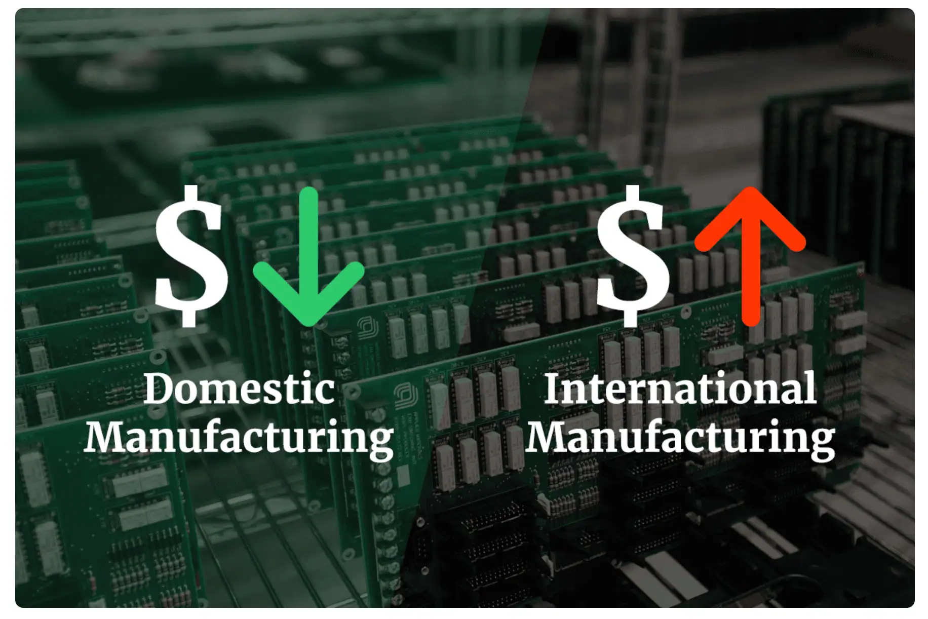
As the global trade tensions continue, designers who have historically relied on overseas manufacturing are beginning to feel the squeeze. The clear-cut cost advantage of foreign production is diminishing as domestic electronic manufacturing becomes a more viable alternative. The daily challenges of supply chain management are becoming more difficult to predict and analyze.
A US-based electronics contract manufacturer (CM) can streamline this process and help you avoid demand spikes for sub-products and raw materials that can lead to budget overruns. VSE combines deep engineering expertise with robust supply chain control. Our manufacturing engineers work closely with the design team to verify design intent before our procurement team leverages a broad base of suppliers for competitive quoting and sourcing redundancy.
Chinese “De Minimis” Loophole Closure
Previously, some overseas purchasers circumvented tariffs by breaking down orders to fall below the $800 “de minimis” threshold for small-order exceptions. This practice effectively traded higher shipping costs and longer lead times for tariff avoidance. However, this loophole officially ended in early May 2025 due to executive orders.
Design teams that relied on this method must find alternative overseas manufacturers or bring production to the United States. The time required to identify and verify new international partners could significantly delay your production schedule. Partnering with a domestic manufacturer like VSE can reduce international turnaround times by more than half while ensuring high quality and simplifying supply chain management from design review through lifecycle management. This allows you to accelerate your products to market and lead your market, not fight to catch it.
Traditional Cost-Driving Factors
While new tariffs and trade policies are adding a layer of complexity to the 2025 landscape, many of the traditional cost drivers in PCB manufacturing remain as relevant as ever. These factors, which are directly tied to the physical design and production process, are where designers have the most control to optimize their costs. Understanding how your design choices, from material selection to layout complexity, impact the final price is essential for a successful and cost-effective project.
Manufacturing Complexity
The thicker the board and the more layers it has, the greater the material and processing costs. Four-layer boards are often considered an unofficial design standard because they strike a good balance between cost and design complexity. Understanding the fabrication process is key: fabricators translate copper designs from ECAD data using acid etching and fuse discrete cores/prepreg materials through lamination.
While etching is a parallel process, lamination is sequential. A single lamination step is sufficient for some designs – through-hole drilling requires only one pass. However, more complex via structures (e.g., blind and buried microvias) require sequential lamination that drills the appropriate layers first before combining the disparate sub-laminations.
These fabrication examples are all cost adders over “basic” work orders. While they may be necessary for complex designs, a design review may be able to limit extraneous or downright unnecessary fabrication processes. Think of it like a “measure twice, cut once” idea: upfront design review between the client and manufacturing engineer can limit these elements, reducing per-board manufacturing costs.
Precision
In general, manufacturing has to navigate the ambiguity of interpreting design documents, while designers want to avoid over-constraints. Designers should begin by recognizing the IPC class of their layout: general consumer electronics are class 1, dedicated service electronics are class 2, and high-reliability electronics are class 3.
These classes represent intensified quality and reliability requirements due to the risk of field failure. Designing a class 1 device to class 3 standards does little for the performance, and the reliability of these devices is less critical due to their rapid obsolescence.
Cost-Prohibitive Manufacturing Tolerances
| Annular rings | Below 6 mils, annular rings can be more prone to breakout (hole perimeter extends beyond pad dimensions), affecting the circuit’s current-carrying capacity and overall reliability, causing board rejection during inspection. |
| Outline dimensions | Below 4 mils, board fabricators will expend smaller, expensive drill bits more rapidly. Keeping the outline simple with straight-line corners can reduce this cost driver even further with V-scoring. |
| Trace width/spacing | Thinner trace widths and gaps are necessary for dense pinout breakout but require specialized processes and equipment. Unless necessary, avoid trace width/spacing below 4 mils. |
| Hole size | Like with the board outline, smaller hole sizes mean smaller drill bits that wear out faster. Additionally, hole size tolerance can increase rejection rates. Hole size precision of or less than 2 mils can be overly restrictive. |
| Aspect ratio | Vias and other through-holes must balance hole diameter against depth: the smaller the diameter, the more likely it is to encounter mechanical failure or plating irregularities that ultimately lead to board scrappage. Holes shouldn’t exceed a 10:1 depth-to-diameter ratio. Microvias are a solution for smaller holes that take less board real estate. |
| Impedance | Controlled impedance lines are necessary in modern electronics to meet the needs of various transmission protocols. Impedance tolerances stricter than 10% may limit manufacturing partners. Poor compatibility between trace requirements and materials can further complicate costs. |
Soft Costs
One of the best ways to reduce soft costs is through an early design review that identifies potential Design for Manufacturing (DFM) or supply chain issues. VSE is a boutique manufacturer with major industry capabilities. Our agile production allows for the rapid implementation of changes and corresponding documentation, keeping production on schedule.
Communicating Design Intent
| Underspecified | Overspecified |
|
|
The Benefits of an Experienced Contract Manufacturer
Understanding the link between cost and quality is crucial. The old motto “Do it right, or do it twice” applies directly to PCB manufacturing. While profitability is essential, elevating it above performance and reliability can damage a brand’s reputation. Poor manufacturing outcomes lead to scrap or rework, which are unnecessary cost adders that jeopardize shipping deadlines.
Partnering with an experienced US-based CM like VSE can get ahead of these issues while offering benefits that overseas manufacturers may not be able to match:
- Expertise for Complex Applications – From medical devices that demand stringent regulatory compliance to semiconductor technologies requiring cutting-edge precision, certain industries leave no room for error. A trusted domestic CM can navigate these complexities, ensuring that boards meet exacting standards without introducing unnecessary delays or costs.
- Managing Total Cost of Ownership – PCB production costs extend far beyond the unit price. Design misinterpretations, long shipping timelines, or excessive rework all add hidden expenses. An experienced CM manages these soft costs proactively through early design reviews, clear communication, and lean manufacturing practices, reducing lifetime project costs rather than just lowering initial quotes.
- Closer Collaboration and Transparency – Touring a local facility or simply having overlapping work hours facilitates more direct collaboration. This transparency accelerates revisions, ensures design intent is understood, and provides confidence in both schedule and quality. At VSE, we protect your IP and act as a true extension of your team.
- Risk Mitigation & Lifecycle Continuity – A skilled contract manufacturer also helps reduce long-term risk by managing part obsolescence, qualifying alternate suppliers, and maintaining clear documentation. At VSE, we actively reduce risk by flagging components that are going end-of-life, offering alternate parts, and building flexibility into your supply chain.
Your Contract Manufacturer for 2025 and Beyond
The uncertainty surrounding 2025 PCB costs is a challenge, but designers can simplify logistics and improve quality by partnering with a local manufacturer. At VSE, our engineers are committed to building high-quality electronics for our customers. We provide a full design review before manufacturing to minimize costs, and are curious to understand and solve your complex challenges. Through coordinated efforts, VSE guides design teams through a confusing supply chain to get their products to market faster and without interruptions.


