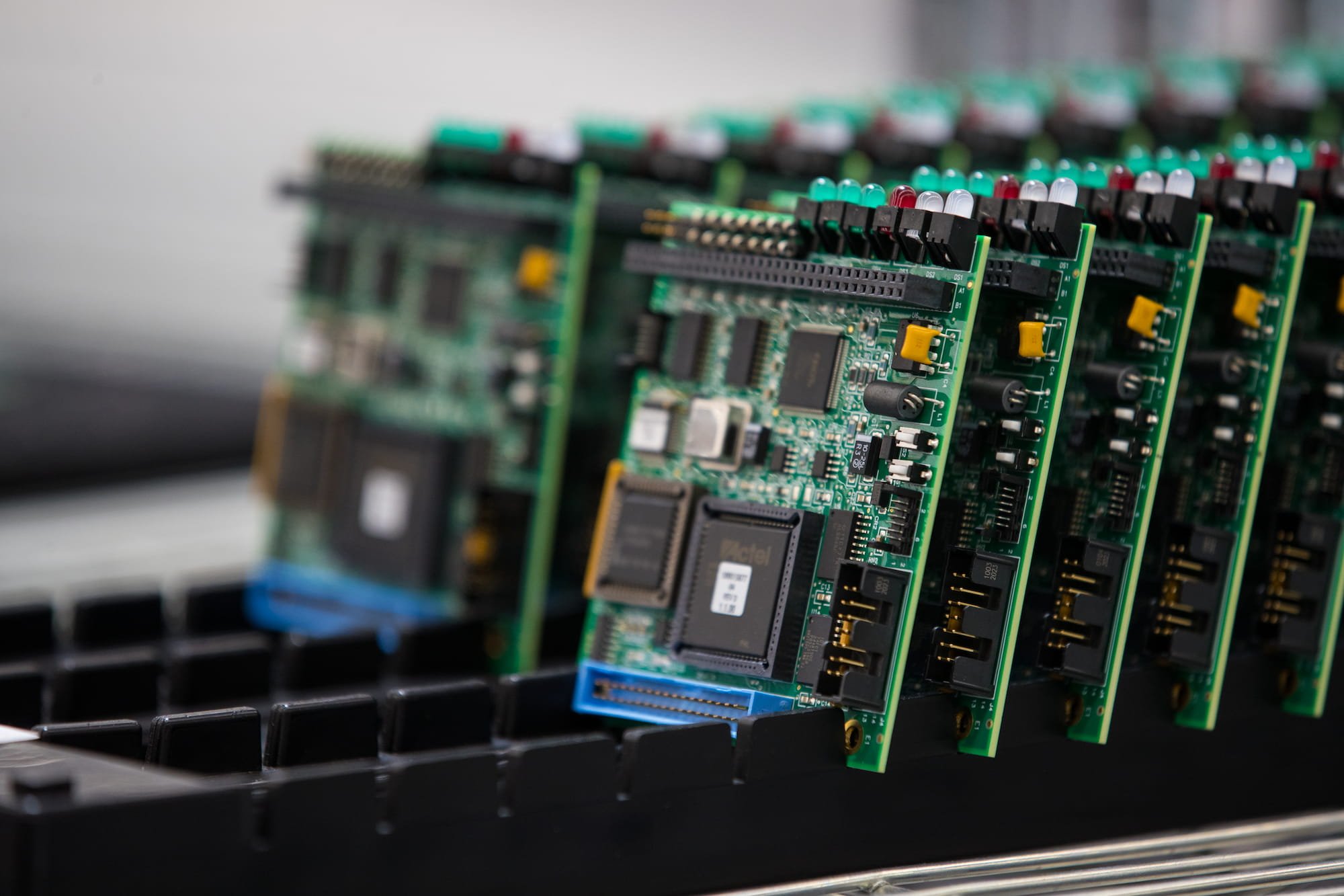
Except for some simple layouts, most of today’s boards use a multilayer stackup to meet the needs of a design while balancing performance. As device functionality has become more all-encompassing, designers must struggle with incorporating more circuitry into less space – especially for portables. Designers will want to partner with an accomplished multilayer PCBA manufacturer to ensure the design intent carries through from schematic to board. At VSE, we’ve been realizing complex designs for life-changing and life-saving devices for over forty years; see the expertise you can expect from our engineering team.

| Multilayer PCBA Manufacturer Recommendations | |||
|---|---|---|---|
| Stackup | Components | Signal integrity | |
|
|
|
|
How a Multilayer PCBA Manufacturer Improves Layouts
How can a manufacturer assist with multilayer PCBA planning?
When placement is tight, procurement teams can aid the layout by seeking equivalent or drop-in replacement components with smaller footprints to free up board real estate. Similarly, swapping SMT components that do not impede inner-layer or reverse-side layouts can relax placement constraints. Reviewing component costs, lead times, and availability will maintain a smooth production timeline that prevents budget and deadline overruns.
Vias come in numerous shapes and applications; all vias have the central goal of providing inter-layer continuity, but how they achieve it noticeably varies. Smaller microvias like blind and buried vias, while a cost-adder to fabrication, can drastically shrink via sizes and are a foregone conclusion in high-density interconnect (HDI) designs. A via-in-pad arrangement leverages the outer layer board area already assigned to landing pads to further routable board area. By communicating with a multilayer PCB manufacturer like VSE at the nascent stages of board development, designers can better incorporate manufacturability and cost concerns for a more seamless transition to manufacturing and final product.
FPGAs (and other highly pin-dense components like BGAs, LGAs, etc.) are synonymous with multilayer PCBA manufacturing due to their vast fanouts and supporting circuitry. However, the size and density of these pinouts can frustrate traditionally cost-effective, probe-based testing methods, leading to cost increases disproportionate to the savings gained from these components. Placing test points on the outer layers electrically connected to the nets under test ensures testing remains rapid, even for mid-to-high volume production lots.
