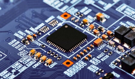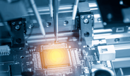
Reflow soldering, a method of attaching SMD components to a PCB, has some similarities: the board experiences a pre-heating section of the oven that ensures the quality of the solder joint formation. In general, the greater process control of reflow soldering affords manufacturers more leeway during the assembly process while reducing the thermal stress and shock introduced to the board.
| Reflow vs. Wave Soldering | ||
|---|---|---|
| Reflow | Wave | |
|
|
|
An Overview of Reflow Soldering
Reflow soldering is the SMD alternative to the through-hole wave soldering technique; instead of a molten wave of solder passing underneath a board and wicking up the leads, a convection oven melts pre-applied solder paste to form the joints. While the wave solder approach has necessary quality controls, reflow is more meticulous as operators can control heating and cooling rates with infrared heating and convection cooling, respectively. Central to this process is the reflow profile, which describes the temperature of the process as a function of time, consisting of a pre-heating warm-up before the boards enter the reflow-temperature area of the oven. This setup is both a necessary function and advantageous; unlike wave soldering, where the board underside is only briefly in contact with the molten solder, boards experience a heightened temperature environment for the length of the oven’s heated portion (this can be around 4 minutes, but exact times vary by model). Calibration of the temperature soak not only minimizes the thermal excursion of the board and components, but the slower run-up to the melting point also minimizes thermal shock.
In total, the reflow profile consists of four distinct zones:
- Preheat – This area of the reflow process is to slowly bring temperatures up to the soak – usually less than (2 ℃/s), but exact values will vary according to the board, solder, and component materials. Preheating prevents cracking due to thermal shock and solder splattering that can lead to shorts.
- Soak – The soak region is an intentional delay between preheating and reflow to ensure the entire board and assembly are at a consistent temperature before reaching the solder melting point. The amount of time a board needs to spend soaking depends on a few factors, primarily the board thickness and how populated the assembly is. A constant temperature across the board eliminates cold spots that can negatively impact joint formation.
- Reflow – The temperature exceeds the solder melting point for a period (usually 30 to 60 seconds) to allow for proper joint formation (i.e., wetting) across the board. There is a delicate balance between insufficient heating time (which leads to cold joints and potentially intermittent continuity errors) and excessive heating time that creates brittle solder joints and can damage some components. Additionally, the atmospheric conditions are a consideration, as reflow temperatures in the presence of oxygen can lead to the formation of oxides that inhibit solderability; process controls may call for flooding nitrogen gas in the heating chamber.
- Cooling – The cooldown period is similarly essential to the preheat period as the various materials quench; an accelerated quench can lead to damage, just like an accelerated preheating. Therefore, cooling should be at a gradual, linear rate (typically ~ 3℃/s) as the boards move toward the end of the reflow oven and exit the process.
Designer Tips to Improve Reflow Assembly
With an idea of the reflow oven operation, designers must address a few items during planning and board layout to aid the process:
- Asymmetrical routing – Especially for smaller components like chip packages, a disparity in the amount of copper connected to the leads can greatly impact the differential heating of the two pads. Improperly managed routing may lead to tombstoning, where the uneven melting rates of the solder on the pads pull the chip component off the slower melting pad, resulting in a discontinuity. Carefully check that the copper connected to chip packages is evenly distributed, including vias.
- Copper balancing – Exposing the boards to high temperatures means a necessary expansion of the board and assembly materials according to their coefficient of thermal expansion, or CTE. Copper and dielectric substrate materials (e.g., FR4) have a noticeable difference in CTE, which can create appreciable thermal stresses during heating and cooling that warp the board and destroy connections to the via barrel. Copper balancing, as much as possible, ensures an even heating profile across the board by keeping copper with no electrical function in areas that would otherwise be empty (physically, this simplifies the etching process, as less etchant reagent is necessary). On the design end, layout designers need only to add no-net copper pours to the design with a corresponding callout or fabrication note on the drawing.
- Component placement – In actuality, outcomes are more dependent on the quality of the pick-and-place machine and any associated vision training. Still, designers can assist the process by using equal component spacing and aligned horizontal/vertical centers for repeatable analysis.
Your Contract Manufacturer Optimizes Soldering for PCBA
Reflow soldering goes hand-in-hand with SMD-heavy assemblies for HDI designs, offering exceptional quality control over wave- and hand-soldering methods. However, this additional level of processing comes with added responsibilities for floor managers: the lengthened time in the reflow oven compared to the alternatives may be incompatible with certain board and component materials. Designers looking to optimize their assembly outcomes can partner with a leading PCBA manufacturer for over 40 years: at VSE, we’re a team of engineers committed to building electronics for our customers. We’ve been proud to realize several life-changing and life-saving products with our manufacturing partners.


