Most people enjoy a sunny summer day, but national weather this year has been punishing for many. A/C has gone from a luxury to a lifeline in some of the hardest-hit areas, underlining the necessity of thermal regulation to prevent heat exhaustion and more threatening conditions. Like a person, a circuit board unprepared to dissipate generated heat will suffer performance losses and experience early aging that reduces the device’s service life.
Fortunately, there are numerous methods designers can employ to actively or passively dissipate heat to ensure reliable function. PCB thermal management significantly improves a board’s performance in the face of excess heat, and designers will have multiple layout tools for a device to thrive instead of withering.
PCB Thermal Management Design Considerations for Best Performance

Conduction of current and heat intertwine in metals: heat and electricity both rely on the movement of free electrons. Thermal conductivity, as defined by the Weidemann-Franz law, increases with electrical conductivity and temperature, partially explaining thermal runaway conditions. While some heat generation is acceptable for the regular operation of a board, too much heat leads to material breakdown and failure. PCB design techniques must limit heat generation or promote thermal routing away from sources to avoid a board overly-susceptible to moderate temperature increases:
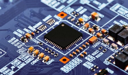
- Component placement – Designers should place components that run hot, such as power parts or microcontrollers, toward the center of the board. This location allows the heat to dissipate evenly through the board instead of concentrating in one region. Provide enough spacing between hot components and neighbors to promote convection to the surrounding air. Consider placing sensitive components some distance from heat sources.
- Traces – Increasing the copper thickness and area coverage by layer will also help to dissipate heat. This modification will have the knock-on effect of increasing the width of the traces as well, providing more volume and surface area to flow, depending on the signal frequency.
- Thermal pads – Heat can conduct through the board using plated holes in thermal pads and vias. These holes distribute the heat to large internal copper pours on ground layers or to the opposite side of the board for an improved dissipation rate.
- Board structure – The printed circuit board acts as a heat sink: the thicker the board, the more thermal energy it absorbs. While standard FR-4 board materials can handle a lot of heat, looking into other board materials, such as polyimides or metal cores, may be necessary for excessive heat generation.
- Cooling devices – Additional thermal options like thermal paste under hot components, heat sinks, and fans aid thermal routing and device cooling.
Design Techniques to Manage PCB Heat During Manufacturing
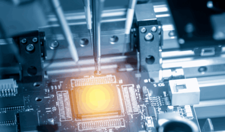
Operational thermal stress is the primary point of thermal management for PCB designers. However, fabrication requires considerable heat and pressure to laminate the layers together. Automated soldering processes, too, introduces thermal stress, either by a wave of molten solder or exposure to a reflow oven.
PCB manufacturing must carefully track materials, components, and process parameters (soak/max temperature, duration, etc.) to ensure:
- Bow and twist – If the metal coverage throughout the different layers of the board is inconsistent, it can cause the board to bow or twist during fabrication due to differences in planar coefficients of thermal expansion (CTE). This imbalance can result in the board warping as high heat and pressure are applied during fabrication. Consider flooding ground pours on layers with minimal copper features, and ensure the stackup is balanced.
- Bad solder joints – Metal around a pin can behave as a heat sink during soldering and robs heat from the joint. As a result, the solder doesn’t melt or wet completely, leaving a cold joint with sub-standard electrical and mechanical characteristics. A thermal relief pad concentrates heat on the junction between the pin and PTH in these cases.

- Tombstoning – Tombstoning occurs when an appreciable thermal imbalance between the two pins of a small chip package lead to differing wetting forces during joint formation. The package lifts off the board away from the pad with insufficient wetting force while the joint sets on the other pad, leaving the component lengthwise perpendicular to the board surface. To prevent this, PCB designers should check that routing to and from chip package pads are identical regarding trace width and via count.
Even with careful design practices, some components are still more susceptible to thermal problems during circuit board assembly than others. Designers should carefully review product datasheets to ensure compliance with all manufacturing processes and expected operating conditions. However, a contract manufacturer (CM) can expedite this process and offer additional insight, including heat shields during and modified soldering processes to prevent sensitive components while reducing manufacturing time and cost.
How Your PCB Contract Manufacturer Can Help You with Thermal Management on your Board
Usually, PCB thermal management issues descend from the power circuitry. A PCB CM will typically review a board’s bill of materials (BOM) first to identify components with high power requirements. The review then triggers a probe of the design to ensure it will meet manufacturing and operating requirements:
- How do the layout and design rules support the expected current and power requirements?
- Is there a preferred airflow direction to cool high-power components? An enclosure designed to optimize heat flow can go a long way to alleviating thermal concerns without requiring any board-level revision.
- Is the part list final, or are parallel prototypes necessary to test potential component changes?
- Are there any sensitive components whose performance may be impacted by being too close to heat sources?
At VSE, we’re a team of engineers committed to building electronics for our customers, including a full assessment of design fitness for its intended environment. Whatever the design requirements, VSE can enhance every aspect of a PCBA’s DFM, from layout to system integration; alongside our valued manufacturing partners, we’ve been building life-changing and life-saving devices for multiple high-tech industries.


