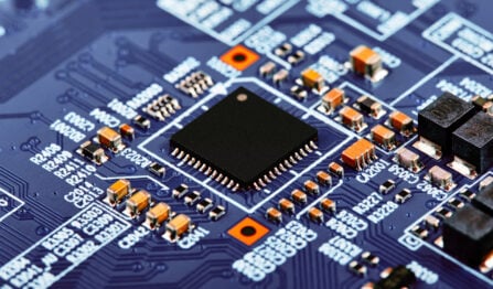
Sometimes, it’s difficult to fully appreciate how small electronic components have become. Even those with familiarity working with breadboards or hand-soldered electronics projects may have no idea that the packaging technology on display there may be several decades out-of-date from modern components. There’s a good reason for this gap. The skills and equipment needed to hand-solder an SMD package are similar to that of a fine jeweler or watchmaker.
The intricate design of printed circuit boards reflects the extremely sophisticated equipment used to manufacture them. Without the abilities of a PCB pick-and-place machine, the improved thermal and power performance of smaller component dies would be meaningless: placement would become impossible or slow to such a pace as to make even moderate production quantities or assembly density unviable. Thankfully, PCB placement machinery, in combination with other manufacturing equipment and practices, has enabled the production of smaller, faster, and more powerful devices.
Did You Know?
In the time it takes an average reader to finish the text in orange (~1 second),
a pick-and-place machine can place nearly 56 components. That’s roughly 200,000 components an hour!
A PCB Pick-and-Place Machine Overview
![]()
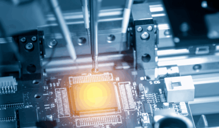
The use of a PCB pick-and-place represents the bulk of the assembly process. While the components will not be bonded to the bare board at this stage – that follows during automated (and manual when necessary) soldering steps, soldering would not have much to go off of if components were not arranged as required by the layout and artwork. For the amount of component volume that a pick-and-place can run through within such a short amount of time, it leads all placement modes with the lowest defect rate; this stunningly-high accuracy results from a visual system that can check and evaluate on-the-fly.
Historically, the pick-and-place machine was motivated by the need for automated placement equipment of surface-mount devices (SMDs). Surface-mount devices can not only be much smaller package sizes than earlier through-hole (TH) technology on the outer layer. The lack of pins through the board also conserves additional routing space on the inner layers that would otherwise be reserved for drilling. As surface-mount technology (SMT) has continued to shrink package sizes to minuscule sizes, the pick-and-place machine also bypasses the logistics issue of manually soldering small devices. While dense assemblies and high-volume production lots would want to avoid manual soldering anyway due to loss of cost and accuracy efficiency, the parallel development of SMT and pick-and-place machines cannot be understated.
Machine placement tends to focus on three central operations:
- Location: The visual system uses high-resolution cameras as the basis for calibration by using fiducials to keep the part placement aligned with the virtual grid used during the layout. These optical systems can also check a design for the absence of a component, swapped component placement, or damage that likely portends current or future performance issues.
- Orientation: A component can be placed within linear tolerances and pass through the soldering process without issue yet still cause unpredictable runtime behavior if the part’s pins don’t feature the same rotation angle as the land pattern pads. The component’s orientation can be measured at pick up and compensated for during placement to ensure alignment.
- Pickup: Heads that can move in three dimensions and rotate, remove, and place parts using pneumatic action. While the moving heads attached to the nozzles are the norm for current and recent generations of pick-and-place machines, earlier machines would move the PCB to fixed-position feeder heads. The continued shrinkage of SMT and sophistication of the pick-and-place technology now allow the PCB to remain fixed while heads move about the board.
Incorporate Design for Manufacture with a Pick-and-Place
Pick-and-place machines are highly precise and sensitive devices, and a quality PCBA is more tied to the correct set-up and operation of the equipment than upstream design. However, the layout can support the placement process by keeping a few ideas in mind:
- Place boundaries/courtyards: Land patterns and design rules may tend to overlook the courtyard because it is not technically a mechanical feature but an extension of the package dimensions. In densely populated boards where every mil counts, designers may overlap place bounds to squeeze out as much layout space as possible. However, overreliance on this tool can result in assemblies that lack reworkability and, in extreme cases, disrupt the operation of the pick-and-place machine. Standard dimensions for place bounds should extend .25 mm/10 mils beyond the x- and y-positions of the component body lines. Include collisions for place bounds in the rules check.
- Board-edge clearance: Placing components too close (typically <1 mm/40 mils) to the board edge can result in poor pick-and-place results due to board flexure (especially for heavier components). Heavier parts near the board edge are also liable to suffer from increased susceptibility to vibration/shock without additional fasteners.
- Package selection: Where substitution is possible, comparable smaller component(s) may be better suited for a pick-and-place assembly due to the packaging of the component order: larger components may not be available as a tape reel, instead using trays that hold fewer components and require quicker replacement. This may not be a concern for low-volume/prototype runs but can bottleneck throughput in large production runs.
The precise nature of the modern pick-and-place machine means that layout placements are unlikely to upset the process, even if the design is suboptimal. However, poor design choices may pop up in other manufacturing areas, like the subsequent wave solder machine. Always remember during design for manufacture (DFM) reviews that no single process exists in a vacuum.
VSE Is the Place to Pick for Contract Manufacturing
A PCB pick-and-place machine is vital for the success of any assembler: its technologies support dense component placements and high-volume production capacity. In tandem with a manual soldering team for large or irregularly-shaped components, a pick-and-place machine offers comprehensive assembly ability for even the smallest devices, improving power efficiency and thermal load. To elevate from design-ready to DFM-ready, a contract manufacturer can greatly expedite the process and smooth out any adjustments or revisions.
Here at VSE, we’re a team of engineers committed to building electronics for our customers. Together with our valued manufacturing partners, we deliver high-quality PCBAs in various life-saving and life-changing industries.


