What Separates PCB vs. PWB?
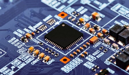
What separates a PCB from a PWB? A PCB is a fully-assembled PWB; to put it another way, every PCB is a PWB, but not every PWB is a PCB. A board is often called a PCB regardless of its assembly status. Although PWB is a bit outdated, most users in the industry would not be overly concerned about the conflation between the two terms. To further complicate the matter, there are explicitly defined terms for an assembled PCB: a PCB assembly (PCBA), a printed circuit assembly (PCA), or the industry-preferred circuit card assembly (CCA).
It’s far more likely that readers would intuitively understand the name “printed circuit boards” if they have some passing familiarity with the industry, but “printed wiring board” is a bit more opaque. Most designers are unfamiliar with wiring at the bare board design stage, and most common associations wouldn’t fit with the term. Wire bonding denotes a semiconductor-specific fabrication process, while processes like wire wrapping and point-to-point construction fall more towards the prototyping end of the design, with the latter falling into extreme disuse except for the term extending to breadboard usage. As it turns out, “wire board” likely originates back to the initial genesis of modern electronic design when Albert Hanson began developing an alternative to telephone switchboards.
Fabrication Leads to PWBs…
The fabrication process to produce a PWB is long and intense. It involves physically binding, stripping, and adding features sequentially, promoting structural integrity and long-term reliability. Material and process selection confers various properties to the final board and must be carefully considered between the design team and fabrication shop.
Broadly, fabrication can be grouped into a few different sub-categories:
- Panelization: A common misconception about manufacturing is that customers are not paying by the board but by the panel. Considering clearances and space for coupons is a more effective use of space; carefully arranging the design throughout a panel results in a more economical production lot.
- Masking: Artwork from the CAM outputs is properly compensated and transferred to the copper foil layers to form a template for the copper features. Generally, the mask is some etch-resistant solution that protects the copper underneath it while placed in an acid bath, though other subtractive methods exist, such as milling.
- Etching: Most commonly, copper layers are submerged in an acidic solution to remove the uncovered copper. This process is not a simple soak. The total immersion time of the board will depend on foil thickness, temperature, circulation of the etchant, and the copper saturation of the solution. These variables must be carefully weighed to ensure design features such as trace widths are maintained.
- Lamination: The disparate layers of the board (cores, prepreg, single-side laminate) are joined together through elevated temperature and pressure. The layup of the layers is important to align the design and prevent registration errors; the accuracy of individual layers can become meaningless when shifted relative to the origin.
- Drilling: Most designs require a connection that runs the board’s width. Drill data generated by the designer after the layout provides instructions for a drill machine, namely where to place the drill and what size hole is required (not including plating). More complicated drill structures than through holes may require a controlled depth drill or even laser-drilled vias.
- Plating: The board undergoes a plating process to create a conductive surface for any plated through holes. Sometimes referred to as “up plating” due to the extra layer of deposition placed on the outer surface of copper features that aim to provide additional reliability. A final plating, known as the surface finish, protects the copper from oxidation and improves solderability.
- Finalizing and testing: The design is sequentially covered with a solder mask (except in the areas meant to be soldered) and has all relevant designators, and otherwise significant visuals applied, typically with a silkscreen process. The board’s fabrication is complete, and all it requires before passing through to assembly is a thorough test of the board’s connectivity.
…While Assembly Outputs PCBs
If the bare board is akin to the construction of a house, assembly is the furnishing process. Turning a PWB into a PCB is a less intensive step than combining and processing materials into the base of the electronics, but don’t be fooled: modern PCB assemblies can require thousands of components, some so small that tens of them can easily fit on a fingertip. Assembly needs to balance speed and accuracy for economic viability. This rule extends backward into component selection, as SMT has rapidly replaced through-hole technology due to size and additional considerations like the associated soldering process.
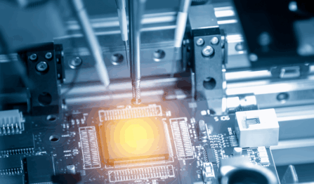
Before soldering, the board’s components must be accurately placed, including the alignment of the package’s rotation with the associated land pattern. This is usually performed with a pick-and-place machine, which can easily populate boards with tens of thousands of components within an hour. Pick-and-place machines can be separated into chip shooters, which are higher volume and less accurate, and flexible placers which have lower throughput but greater accuracy. Roughly speaking, the accuracy of a device, and its associated placement technology, can be sorted as shooters for passive and flex for active.
The board must undergo a soldering step to fuse components to the board once they are set in place. The style of the process and the total number of soldering passes will depend on whether the components are SMT, through-hole, or a mix of the two. For SMT, the board runs through a reflow oven to melt the tacky solder paste that temporarily holds components in place into a more lasting bond. Wave soldering, on the other hand, has a molten wave of solder flow across the underside of the board, joining solder to a through-hole pin and its surrounding pad.
The final step of assembly, like fabrication, is testing. Assembly tests are more in-depth than fabrication because integrating electrical components with the bare board changes the underlying parameters under consideration. These tests must determine not only the quality of the placement and soldering but also the overall functionality of the board – does the design perform what it purports to do?
Whether Bare Boards or Assemblies, Your Contract Manufacturer Has You Covered
PCB vs. PWB is less of a competition and more of an understanding of how two entirely different yet complementary processes combine to create the electronic devices that permeate consumer and industry devices. Many of the modern world’s marvels and conveniences arise from an exceedingly complicated manufacturing industry that has continuously honed itself for most of the last century. Yet the current pace of development continues to push electronics – and production – to tighter tolerances and new challenges. Whether it’s prototyping or mass production, you need a contract manufacturer who is well versed in the current design methods and is at the cutting edge of technology. We at VSE are here to help! We’re a team of engineers committed to building electronics for customers, and with our manufacturing partners, we strive to deliver a board of the highest quality.


