“Measure twice, cut once” is the guiding mantra to prevent irreversible mistakes during any manufacturing process. However, no matter how many eyes check a document or process, some defect or error eventually sneaks through. Luckily, not all errors are equally disruptive, and focused efforts on the primary modes of failure or performance issues can prevent complete malfunction. Establishing and communicating clear design intent also helps prevent ambiguity from sneaking into production, reducing the possibility of issues arising.
Make no doubt that modern PCB design is collaborative, complex, and intensive. Eliminating common PCB problems before a board enters fabrication or assembly processes will drastically reduce costs and improve turn time associated with reproduction.
Combatting EMI From the Ground Plane Up
Fabrication is the broad combination of manufacturing steps that occurs before the completion of the bare board product. Fabrication is more intensive in terms of the board’s stresses and the total number of processes than assembly. Intuitively, this should make sense, there’s more work to be done on providing the physical form and features of the board. Many fabrication processes are decided well in advance, as the design must properly synthesize the features and properties of materials to reach desired performance levels.
An area of particular concern to designers and manufacturers is alleviating EMI through a combination of material and design choices. All boards are subject to EMI testing, but high-speed designs, particularly, are highly susceptible to failure due to signal propagation speed. Regardless of the type, any board failing EMI control tests will be sent back to the revision stage, a potentially disastrous event when trying to meet tight time-to-market benchmarks.
With proper foresight, EMI challenges can be properly anticipated before production begins:
- Material selection. A board inherits most of its properties from the material or materials used as prepreg. Designers might be familiar with distinguishing materials based on the dielectric constant (Dk) and loss factor (Df), which are responsible for electrical susceptibility and inherent heat dissipation. Neither of these properties exists statically – both scale with increasing frequency of the propagating wave, causing greater energy loss. Fabricators and designers should have a dialog before any layout as to which materials will meet the criteria set forth by engineers or manufacturers’ datasheets.
- Routing. Short and direct traces behoove the designer for both signal integrity and HDI. This also extends to return paths: the smaller the current loop, the better the field containment (up to maximum material ratings). Avoid routing over split planes, which can lead to extreme EMI emissions as a signal has to create a much larger and circuitous current loop. Except for a paired differential signal, beware of routing high-speed traces in parallel over long distances, as this can lead to coupling between the lines.
Common PCB Problems During Assembly Are Contested in Layout
Errors occurring in assembly can be more costly than fabrication due to the amount of processing the board has undergone to reach the former. The underlying issues driving assembly defects are among some of the simpler errors to correct when detected, adding to the frustration when these design oversights make their way to manufacturing.
Acknowledging the following issues during placement and layout can greatly improve the immediate and long-term reliability of the solder joint bonds:
- Part verification. Issues in the land pattern design can manifest at this stage if components cannot solder down due to mistakes in the dimensioning. A common mistake is creating a land pattern with the wrong package.
- Shadowing. Consider lead orientation relative to the direction of the solder wave. Having leads positioned perpendicular to this direction of the solder wave will help prevent solderability issues due to the package’s cast “shadow,” disrupting the solder flow path. Short components should not be placed too close behind taller components for the same reason.
- Tombstoning. A process by which parts are lifted off of one land due to unequal wetting forces during solder reflow. The freezing of the solder joint can further lift the component off the board, sometimes resulting in a position normal to the plane of the board. For chip packages and similar two-pad land patterns, ensure that land patterns are appropriately sized and spaced to promote proper adhesion between solderable pads.
- Double-sided assemblies should be rejected whenever possible in favor of single-side assemblies to prevent additional heat exposure to the board.
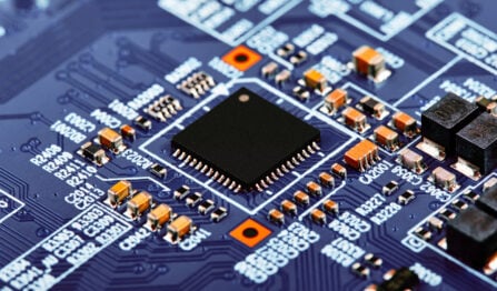
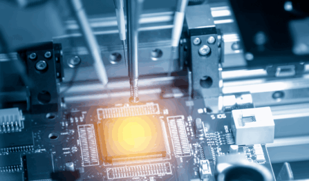
Successful soldering also relies on the correct position and rotation of parts during the placement. One of the most overlooked design elements necessary for assembly is the fiducial. Its generation and placement take little more than a few minutes, but its effect on the success of assembly is hard to overstate. Fiducials assist with computer vision, acting as targets for pick-and-place machines and other highly autonomous equipment. Fiducials are typically placed in groups of three, with each additional fiducial upgrading the accuracy of the vision:
- Assesses x- and y-location in the plane.
- Determines board rotation in the plane.
- Measures stretch/shrink in the plane due to thermal and mechanical stress/relaxation equilibria.
These global fiducials affect the placement of all parts on the board, but parts requiring more precise alignment due to high pin count, such as BGAs, may possess their own local fiducials.
Your Contract Manufacturer Can Navigate Production Challenges
PCB manufacturing is rife with the possibility of defects arising from the design. Even with robust design rules and extensive verification steps, the likelihood of encountering common PCB problems will always be nonzero. However, the best design teams can avoid the most debilitating production issues through experience and communication. When you’re looking for a job to proceed smoothly and have a reliable board reach end users quickly, VSE is standing by and ready to assist. At VSE, we believe in a simple philosophy: we’re a team of engineers who build electronics for our customers. Coupled with our manufacturing partners, we aim to deliver a high-performing board, every design and every time.


