When observing teachers working with small children in a virtual classroom, it’s evident that larger groups of children, especially those assembled in the same workspaces, can easily distract each other. Other children’s noise and activity level often causes too much interference and will detract from a child’s instruction. Online teachers adjust the virtual classrooms’ guidelines, encouraging separation between children during class time for a thriving learning environment.
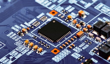
In circuit board design, it is also vital to include separation—and just as with the virtual classroom—the motivation is to lessen interference. With all of its activity, a circuit board can be a hostile environment for sensitive digital and analog signals. It is critical for the overall performance of the board to provide functional partitioning in the PCB design. Here are some ideas on how this can be done in your next circuit board layout.
Functional Partitioning in PCB Design Starts with Component Placement
As with any PCB layout, the path to a good design starts with good component placement. Poor component placement can lead to a lot of corrections later on. But before a good floor plan for the component placement can be devised, the basic circuit partitioning needs to be decided. The board’s size and the required placement of connections, switches, and other interfacing hardware will set the board’s component placement’s initial parameters. After that, the components should be placed according to the functional partitions of the board.
A functional partition’s basic purpose is to separate the board’s digital, analog, and power areas. This geographical separation is necessary to prevent signal interference from occurring between functional sections. The problem is, you can’t just throw all the analog parts on the left side and then all of the digital parts on the right to keep them separated. In a mix-signal board, these parts will have to communicate with each other. An effective plan requires that functional be done interactively with good component placement practices like the following:
- Keep sensitive analog and digital areas of circuitry isolated.
- Isolate power supplies from sensitive components.
- Large components such as processors and memory devices should be placed away from the board’s edges to dissipate their heat better.
- These same components need to be placed close to their interfacing connectors for a smooth logic flow.
- Associated circuitry needs to be placed next to facilitate short and direct high-speed or analog signal routing.
A good floor plan of component placement depends on well-developed functional partitions. Simultaneously, developing the most optimal functional partition depends on how the parts will be floor-planned. This sort of thinking may sound confusing to the rest of the world, but it’s just another day in the office for PCB designers. To keep things interesting, let’s throw in some routing requirements:
PCB Trace Routing Also Needs Functional Partitioning
The best routing strategies are always dependent on how the components are placed. This is why layout designers have always considered the routing while they are placing parts on the board. With functional partitioning of critical areas of circuitry, keeping sensitive traces isolated from other noisy circuitry effects becomes even more critical. Here are some routing considerations to keep in mind while planning out your functional partitions:
- Plan out your layer stackup accordingly for controlled impedance routing and stripline configurations.
- Make sure that there is plenty of room for routing large data and memory buses.
- Provide enough routing room for spacing between sensitive signals such as differential pairs.
- Do not allow routing of sensitive analog traces through digital areas of circuitry or digital lines through analog areas.
Perhaps one of the most common causes of electromagnetic interference (EMI) in printed circuit boards is how the power delivery network is designed. The PDN needs to be carefully planned along with the functional partitions to ensure that all components are receiving enough clean power to handle their requirements. Simultaneously, the design of the PDN also has to consider the circuitry’s needs for clear signal return paths. Here are two critical concerns for the PDN when developing your functional partitions:
Don’t mix the power and ground of different areas of circuitry
The noise created by one area of circuitry, such as a power supply, can be devastating for digital circuitry. Power supplies usually should have an area of the power and ground planes isolated for their use, just as the digital and the analog regions of the planes should be separated. These areas often should be tied together, but they should be connected at only one point to avoid the creation of any unintentional antennas that could radiate EMI.
Avoid the use of split planes, and exercise caution when routing traces nearby
A split plane is often used to consolidate the circuitry and reduce the layer count of the circuit board. For sensitive signals, a split plane can create a lot of EMI by blocking that signal’s clear return path on the reference plane. If you are using split ground planes in your board, make sure you do not route traces across the split. If a trace needs to cross from one area to another, route it across the point where the two ground splits are connected. This will give that signal a clear return path across the split planes.
Functional Partitioning for Thermal Considerations and Ease of Use
It may seem that carefully developing a functional partition plan for a circuit board will ensure its success, but there’s more to consider. The partition and floor plan of the component placement needs to consider the cooling of the circuit board, especially for those boards using parts that run hot. You need to ensure that tall components such as large capacitors don’t block the airflow to other board areas. Also, a hot area of circuitry in one partition may create problems for other areas forcing you to relocate them.
There is a lot to consider when you devise the functional partitions for the component placement on a circuit board. Here is where the expertise of your PCB contract manufacturer can be of great assistance. An experienced CM has built many boards for every kind of PCB technology and has a great understanding of their different needs and requirements. Not only will their engineering staff have a thorough knowledge of PCB design, but their experience will give them the in-depth empirical understanding that you will need for success.
At VSE, our engineers have been working with customers like you for over 30 years. We understand when and when not to isolate analog and digital grounds in a PCB layout to ensure that your high-speed signal return paths are clean. Let us work together with you on your next design and help develop the best functional partition plan possible for your circuit board.


