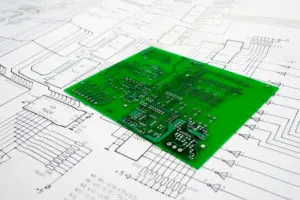
We are so used to the convenience of the different devices and products in our lives, that it becomes second nature to view them only as a completed object. The truth though is that there is some sort of design process involved in their creation, and depending on their complexity, that process could be extremely intricate. Take a smartphone for example. They may look simple on the outside, but inside their complex technology requires a very intricate creation process, especially the printed circuit board that is at their core.
Before a circuit board is manufactured, it goes through a very involved design process. This includes creating an electronic schematic, setting up and placing component footprints in the physical PCB layout, routing the nets in the layout, and then finally preparing and sending out the layout data for manufacturing. In this first of a four-part series, we are going to give you an overview of the entire PCB design process and discuss some of the PCB design best practices for creating an electronic schematic.
The PCB Design Process in a Nutshell
The PCB design process will first start with the specifications laid out by the product development team. These will include what the board is needed for, its performance specifications, its physical size, etc. Once those are in place, the PCB design process will begin:
Circuit Development
Using the product specifications, the engineering team will develop the circuitry of the board by creating an electrical schematic. This includes choosing the required electronic components for the circuitry and placing symbols on a CAD schematic to represent those components. From those components, nets will be drawn in to connect the component pins together to complete the circuitry. Finally, the circuitry will be verified using simulation tools.
PCB Layout
With the connectivity data from the completed schematic, the physical design of the printed circuit board will begin. First, the design team will create or download the correct component models, or footprints, to match the symbols used on the schematic. Then the database will be prepared with the physical outline of the board, the configuration of the layers in the board, and the required design rules. Now the PCB CAD footprint models can be located on the board layout using the connectivity mapped out in the schematic as a guide for the most optimum component placement.
PCB Routing
Once the parts are all placed on the board in the PCB design CAD system, the nets connecting the pins together in the schematic can be physically routed in. The first step is usually to provide “escape” routing from fine pitch surface mount parts. These traces and vias must be strategically placed so as to not block up routing channels on the inner layers, while at the same time providing connectivity for all the pins. Next comes the delicate routing of high-speed transmission lines, differential pairs, impedance controlled traces, analog nets, and other sensitive signals which must be routed according to strict performance rules. After that, the power and ground will need to be routed with wider traces, solid metal plane layers, or split planes. Much of this routing can be done with automatic CAD tools such as batch auto-routers, auto-interactive routers, clean-up routers, while the rest is done manually. Lastly, the routing will need to be verified with different analysis tools.
Design Completion
While the design may be placed and routed at this point, there are still some important jobs left to do. First, the design must be run through its final design rule checks to ensure that there aren’t any electrical shorts, opens, or other electrical or manufacturing problems. This includes mechanical verification as well with 3D tools if possible. Next, the silkscreen markings, solder mask, and solder paste markings from the PCB CAD footprint models will all need to be reviewed, edited, and cleaned up. Finally, the manufacturing drawings will need to be created as well as the fabrication and assembly data, in order for the design process to be completed.
As you can see, there are four main steps to the PCB design process. To start with, let’s look at some good design practices for schematic capture.
The Eight PCB Design Best Practices for Good Schematic Capture
Here is a list of good design practices when capturing a schematic. Note that this isn’t a how-to list of doing schematic capture, that would be dictated by the tools and the actual design. Instead, these are little gotchas that if ignored can potentially cause serious problems for the completed design:
1. Symbol libraries: Make sure that the schematic symbols that you are using are up-to-date, and are the correct symbols for the parts you are using. They also need to have the correct properties and attributes in them for simulation and PCB layout.
2. Circuit flow: Use a consistent logical flow of circuitry so that your schematic is easy to follow and interpret.
3. Real estate: Don’t be afraid to use more than one sheet as there isn’t any reason to cram everything onto one page. At the same time, sheet consolidation is a good thing and your layout, test, and field engineers will appreciate not having to continually jump from page to page to page when working in the schematic.
4. Readability: Make sure that your symbols and text fonts are large enough to be clearly read without taking up too much room. It is also a good idea to establish some documentation standards for your design department if you don’t already have them so that your schematics all appear similar.
5. Legibility: In the same vein, make sure that your reference designators, net names, and pin markings are not merged with other shapes or text so that they are easily readable. It is also a good idea to include design notes to clarify important points for PCB layout and other users of the schematic.
6. Organization: Give your symbols enough room around them and make sure that they are organized in such a way that they are easily identifiable. Use this same rule of thumb when drawing in nets from pin to pin so that you don’t end up with a mess of lines. There are usually many features in the schematic capture tools that can help with this. These include net labels that will virtually join two pins together without a drawn net and net group lines that can hold multiple nets of a bus.
7. Information: The schematic is also a legal and traceable document, so be sure to include all of the pertinent part and revision numbers, as well as the date, company contact, and copyright information.
8. DRCs: Make sure to use the design rule checking in your CAD tools to catch problems such as one-pin connections, or shorted nets.
Another good design practice is to use circuit simulation tools if you have those available. This can save you time in your prototype builds by finding obvious design problems before you go out for manufacturing.
How Your PCB Contract Manufacturer Can Help with the Design Process
One of the best things that you can do to help yourself with your PCB design is to partner early with your PCB contract manufacturer. The PCB CM will have many resources that you can put to work for you, such as additional engineering and documentation personnel to take some of the burdens off of you so that you can focus on the design. In addition, they will have component sourcing experts who know and understand the PCB component supply chain. This can save you hours of extra work trying to find the best supplier of the parts that you need.
At VSE we have been working with engineering teams like yours for several decades now, and we understand the different challenges that you are facing with PCB design. We have a dedicated engineering staff that is ready to work with you to get your board into a manufacturing-ready state. We can help you with design for manufacturability (DFM) reviews, component research and purchasing, and of course, schematic capture and documentation.
If you are looking for a CM that prides itself on its care and attention to detail to ensure that each PCB assembly is built to the highest standards, look no further than VSE. Contact us today to learn more about partnering with us for your next project.

