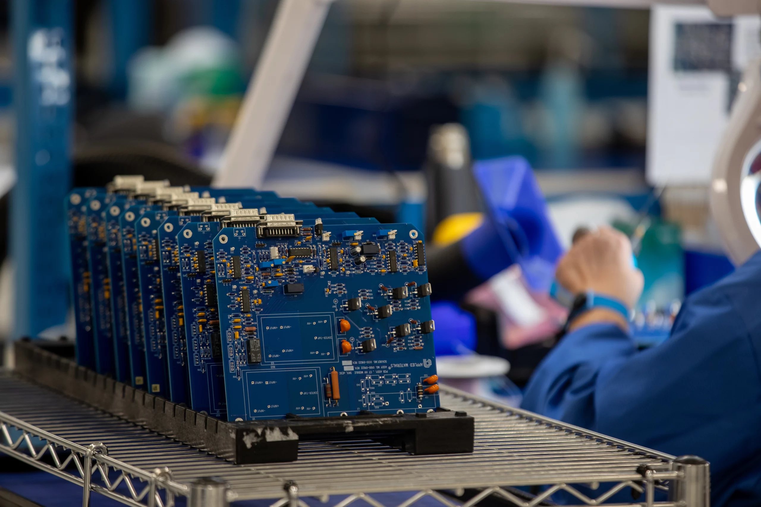
Make no mistake: PCBA design is initially a challenging design task. After all, whole industries are necessary for the software that supports designers in bringing a schematic to life based on input from engineers and manufacturers’ datasheets. Like any new task, breaking up the lengthy and seemingly convoluted process into bite-sized pieces is best. This PCBA design guide looks over the entire design process, from schematic to final documentation, to discuss general guidelines for new designers to avoid common early pitfalls.
Schematic and Land Patterns

Methods of Land Pattern Creation |
|||
|---|---|---|---|
| Component Wizard | Creation By-Hand | ||
Enter the relevant package dimensions (provided by the manufacturer’s datasheet) to build a footprint for common packages. |
Use the manufacturer’s dimensions to design the footprint layers by hand. This approach is more involved and time-consuming than entering common dimensions for a package, but it allows designers to build nonstandard land patterns. |
||
Verify package dimensions (body, pad size, etc.) |
Verification must also be more thorough since checkers can’t assume package details. |
||
Components in preferred packages may be unavailable, and alternate replacements may be necessary. There isn’t much designers can do to circumvent this process, but luckily, updating the BOM assembly information via netlist associations at the schematic level is possible. Designers can even be proactive and create alternate part land patterns for components, such that implementation only requires the association mentioned above and any minor routine cleanup.
The Dual Role of the Stack-Up in Design

While many variables are in play, including the choice of substrate material, the trace factors most directly influencing the impedance will be the trace width and the dielectric height. The trace width can be misleading, as the acid etching will form a trapezoidal shape due to the solution having more contact with the upper sides of the trace as it works around the etch protectant. The base of the trace is always wider than the top, and manufacturers’ datasheets often report this value as the “singular’ width of the trace (in reality, the top width will be about a half-mil shorter).
Building the impedance profiles is only half of the stack-up usage. The designer will want to begin planning how they will distribute power planes, ground planes, and routing planes throughout the stackup to maximize signal and power layers while keeping reference plane distance to a minimum. Distribution should be balanced — think of the innermost core as a double-sided mirror. This method will not work for every design — sometimes, it may be necessary to borrow a plane layer for signal or vice versa, but it will often provide an excellent starting point.
Routing planes should always have an adjacent ground plane on one side for reference. Most designers will insert ground planes on layers two and the second-to-last layer to reference the outer-layer signals, an internal power plane or signal layer on layers three and the third-to-last layer. This stack-up monomer will continuously repeat on larger boards, though power or routing design needs may cause slight deviations.
PCBA Design Guide for Placement and Routing

Providing Clear and Concise Documentation

A Contract Manager For All PCBA Design
Contact us today to learn more about partnering with us for your next project.
If you are looking for a CM that prides itself on its care and attention to detail to ensure that each PCB assembly is built to the highest standards, look no further than VSE.