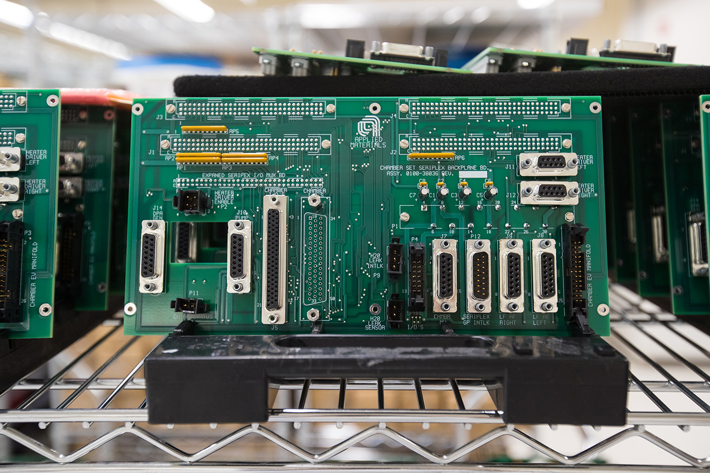
Working with high-speed PCBA designs can add an extra layer (no pun intended) of complexity to your board. Foolproof techniques at low speeds can become unreliable with faster rise/fall times inherent to digital systems. However, these problems are not insurmountable: an experienced high-speed PCBA manufacturer can navigate potential issues at the board level and throughout manufacturing to limit their deleterious impact. With over forty years of experience in cutting-edge PCBA designs, VSE can ensure your design is manufacturing-ready throughout product development.

| Analyzing Design Elements with a High-Speed PCBA Manufacturer | |||
|---|---|---|---|
| Objective | Challenge | Solution | |
Trace |
Connect two or more pins of a design for electrical continuity. |
Adds inductance and capacitance. |
Exchange lossy FR4 material for high-speed substrate. |
Plane pour |
A power or reference plane that acts as a high-frequency capacitor. |
Stray capacitance on signal traces. |
Avoid grid/hatched planes for minimal inductance. |
Via |
Interplanar connectivity. |
Adds inductance and capacitance. |
Minimize via usage as much as possible. |
In the old days of PCBA design and manufacturing, continuity was king – speeds were low enough that there was no need to worry about changes in performance. Signal speeds were so slow relative to today’s numbers that the board was essentially a passive element from a design perspective. No longer: signal speed propagation is significant enough that failure to account for its effects can ultimately scrap a board.
Interestingly, the most pronounced effect of high speed has nothing to do with the layout explicitly. The board substrate – the material that provides insulation and rigidity to a standard board profile – encounters greater losses and timing delays as signal speeds increase due to its anisotropic nature, which affects signal propagation. The glass fiber weave and epoxy resin typical of FR4s and similar laminates differ enough in electrical characteristics that signals traveling fast enough will have different speeds through them. The nonhomogeneity of the material distribution produces an anisotropy that can make signals superficially appear to have identical electrical backgrounds that are considerably distinct. Even the weight and size of the copper encounter challenges at high speeds due to the skin effect that concentrates current toward the conductor’s surface.
Material Considerations for a High-Speed PCBA Manufacturer
FR4 is less than ideal for many high-speed designs; alternative substrates with lower dielectric constants improve signal propagation speeds and curtail loss (while limiting thermal dissipation). PTFE (AKA “Teflon”) is an excellent high-speed solution, although it does encounter some processing issues during manufacturing. Ceramic substrates can also offer improved high-speed performance with fewer manufacturability concerns than PTFE.
Typically, laminates use rough copper on the bonding side (i.e., the substrate-facing side) to improve the adhesion between copper and substrate after lamination. However, the roughness contributes to a higher impedance and greater losses at high speeds as the skin effect prevents current from flowing through the copper and forces it to travel along the surface. Using a low-profile copper laminate minimizes the skin effect, but the reduced adhesion can be an issue for certain substrate materials like PTFE.
